News
New Publication “Nanoscale refractory doped titanium nitride field emitters”
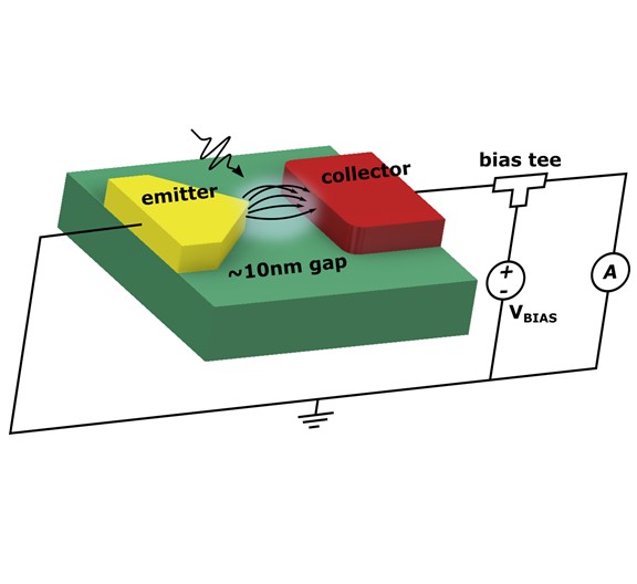
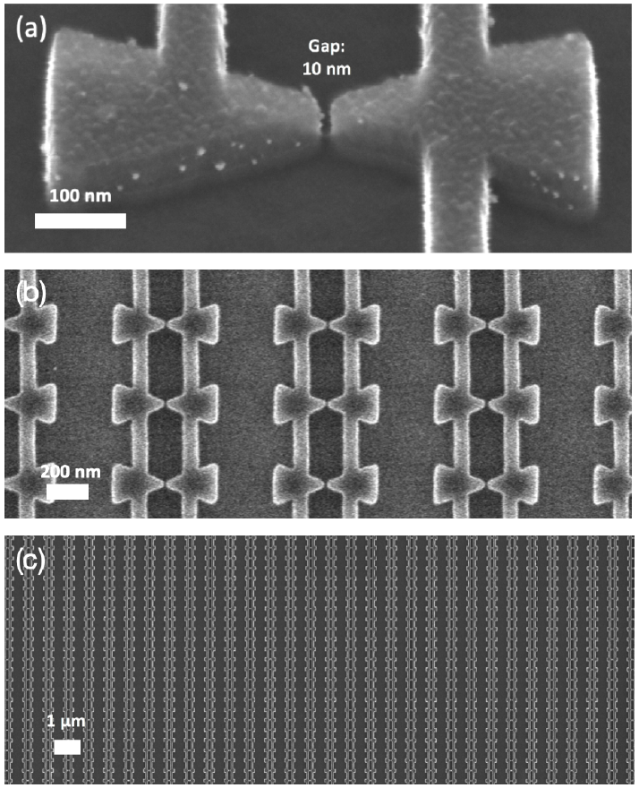
Refractory materials exhibit high damage tolerance, which is attractive for the creation of nanoscale field-emission electronics and optoelectronics applications that require operation at high peak current densities and optical intensities. Recent results have demonstrated that the optical properties of titanium nitride, a refractory and CMOS-compatible plasmonic material, can be tuned by adding silicon and oxygen dopants. However, to fully leverage the potential of titanium (silicon oxy)nitride, a reliable and scalable fabrication process with few-nm precision is needed. In this work, we developed a fabrication process for producing engineered nanostructures with gaps between 10 and 15 nm, aspect ratios larger than 5 with almost 90° steep sidewalls. Using this process, we fabricated large-scale arrays of electrically-connected bow-tie nanoantennas with few-nm free-space gaps. We measured a typical variation of 4 nm in the average gap size. Using applied DC voltages and optical illumination, we tested the electronic and optoelectronic response of the devices, demonstrating sub-10-V tunneling operation across the free-space gaps, and quantum efficiency of up to 1centerdot10-3 at 1.2 μm, which is comparable to a bulk silicon photodiode at the same wavelength and three orders of magnitude higher than with nearly identical gold devices. Tests demonstrated that the titanium silicon oxynitride nanostructures did not significantly degrade, exhibiting less than 5 nm of shrinking of the average gap dimensions over few-μm2 areas after 10 hours of operation. Our results will be useful for developing the next generation of robust and CMOS-compatible nanoscale devices for high-speed and low-power field-emission electronics and optoelectronics applications.
A complete description of the work may be found here.
New Publication “On-chip sampling of optical fields with attosecond resolution”
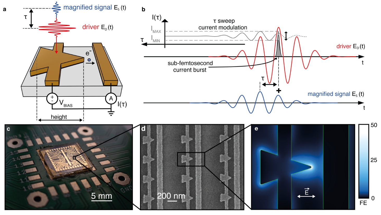
We demonstrate an on-chip, optoelectronic device capable of sampling arbitrary, low-energy, near-infrared waveforms under ambient conditions with sub-optical-cycle resolution. Our detector uses field-driven photoemission from resonant nanoantennas to create attosecond electron bursts that probe the electric field of weak optical waveforms. Using these devices, we sampled the electric fields of ~5 fJ (6.4 MV m−1), few-cycle, near-infrared waveforms using ~50 pJ (0.64 GV m−1) near-infrared driving pulses. Beyond sampling these weak optical waveforms, our measurements directly reveal the localized plasmonic dynamics of the emitting nanoantennas in situ. Applications include broadband time-domain spectroscopy of molecular fingerprints from the visible region through the infrared, time-domain analysis of nonlinear phenomena and detailed investigations of strong-field light–matter interactions.
A complete description of the work may be found here.
Owen Medeiros awarded NDSEG fellowship
Congratulations to Owen Medeiros on receiving the National Defense Science and Engineering Graduate Fellowship. This prestigious and competitive award will support his work for three years.

Emma Batson and Owen Medeiros awarded NSF fellowship
Congratulations to Emma Batson and Owen Medeiros on receiving the National Science Foundation Graduate Research Fellowship. This prestigious and competitive award will support their work for three years.
 a
a
New Publication “Impact of DC bias on weak optical-field-driven electron emission in nano-vacuum-gap detectors”
In this work, we investigate multiphoton and optical field tunneling emission from metallic surfaces with nanoscale vacuum gaps. Using time-dependent Schrödinger equation (TDSE) simulations, we find that the properties of the emitted photocurrent in such systems can be greatly altered by the application of only a few-volt direct current (DC) bias. We find that when coupled with expected plasmonic enhancements within the nanometer-scale metallic gaps, the application of this DC bias significantly reduces the threshold for the transition to optical-field-driven tunneling from the metal surface, and could sufficiently enhance the emitted photocurrents, to make it feasible to electronically tag fJ ultrafast pulses at room temperature. Given the petahertz-scale instantaneous response of the photocurrents, and the low effective capacitance of thin-film nanoantenna devices that enables <1fs response time, detectors that exploit this bias-enhanced surface emission from nanoscale vacuum gaps could prove to be useful for communication, petahertz electronics, and ultrafast optical-field-resolved metrology.
A complete description of the work may be found here.