News
QNN Newsletter from IAP 2026
Dear QNN Group Members, Alums and Affiliates,
Hope everyone is enjoying the start to Spring! We are excited to share updates from the QNN group over the last months.
It has been a while since our last newsletter, so a lot of activity to report. In particular we want to highlight that Dip Joti Paul received the 2026 Claude Shannon Award from RLE, and Adina Bechhofer the 2026 Samsung Semiconductor Fellowship from EECS. Also, last November we held our annual group retreat at Endicott house and have included a picture from the event. As usual, we provide a quick summary of comings and goings, awards, research activity and events below.
Best regards,
Karl and Donnie
Comings and Goings
The last few months we’ve welcomed the following new group members:
- Dong min Kim, Visiting Scientist
- Zhenyang Xiao, Postdoctoral Associate
- Eileen Xiu, UROP
- Jaden McKee, UROP
- Berkan Tarak, UROP
The following members have now left and become alumni group members:
- Josh Piety, UROP, graduated!
- Hanson Nguyen, Undergrad researcher, MSRP
- Giorgia Ciuffarella, Polytechnic of Turin & École Polytechnique Fédérale de Lausanne, graduated!
- Gabriel LeGuay, Federal Polytechnique School of Zurich, graduated!
- Owen Medeiros, working as a Superconducting Electronics Architect at MIT Lincoln Lab
Awards
- Dip Joti Paul has received the 2026 Claude E. Shannon Award!
- Adina Bechhoffer has received the Samsung Semiconductor Fellowship!
Theses!
G. Ciuffarella, “Infrared-Enhanced Electron Emission from Nanoantennas for Optical Detection,” Ecole Polytechnique Federale de Lausanne and Massachusetts Institute of Technology, 2025.
G. Le Guay, “Reconfigurable superconducting logic gate: From photon-driven operation to electro-optic modulation,” Master’s Thesis, Swiss Federal Institute of Technology, Zurich and Massachusetts Institute of Technology, 2025.
Publications (6/1/25-1/31/26)
R. A. Foster, S. Kandeh, O. Medeiros, A. Simon, M. Castellani, and K. K. Berggren, “Time-tagging data acquisition system for testing superconducting electronics based on an RFSoC and custom analog frontend,” J. Inst., vol. 20, no. 09, p. P09018, Sep. 2025, doi: 10.1088/1748-0221/20/09/P09018.
R. Jing et al., “Bolometric Superconducting Optical Nanoscopy (BOSON),” Phys. Rev. X, vol. 15, no. 3, p. 031027, Jul. 2025, doi: 10.1103/f13d-dpdn.
V. Karam et al., “Parameter extraction for a SPICE model of an hTron superconducting thermal switch,” Phys. Rev. Appl., vol. 24, no. 2, p. 024020, Aug. 2025, doi: http://dx.doi.org/10.1103/jdzc-7l2x.
O. Medeiros et al., “A scalable superconducting nanowire memory array with row–column addressing,” Nat Electron, pp. 1–9, Jan. 2026, doi: 10.1038/s41928-025-01512-0.
H. Nguyen, A. Simon, R. A. Foster, and K. K. Berggren, “Modeling electrothermal feedback of superconducting nanowire single photon detectors in SPICE,” IEEE Trans. Appl. Supercond., vol. 35, no. 9, pp. 1–5, Dec. 2025, doi: 10.1109/TASC.2025.3625542.
D. J. Paul, T. X. Zhou, and K. K. Berggren, “Determination of mid-infrared refractive indices of superconducting thin films using Fourier transform infrared spectroscopy,” Appl. Phys. Lett., vol. 126, no. 25, p. 252601, Jun. 2025, doi: 10.1063/5.0268308.
D. J. Paul, T. X. Zhou, and K. K. Berggren, “Photolithography-compatible three-terminal superconducting switch for driving CMOS loads,” Phys. Rev. Appl., vol. 24, no. 2, p. 024060, Aug. 2025, doi: 10.1103/261b-37xx.
F. Ritzkowsky, M. Yeung, G. L. Dolso, L.-T. Chou, and P. D. Keathley, “High-repetition rate, CEP-stable shortwave infrared source with two-cycle pulses for field-resolved spectroscopy,” J. Opt. Soc. Am. B, JOSAB, vol. 43, no. 1, pp. 207–212, Jan. 2026, doi: 10.1364/JOSAB.580422.
Z. Scherübl et al., “Multimode Operation of a Superconducting Nanowire Switch in the Nanosecond Regime,” ACS Nano, vol. 19, no. 32, pp. 29207–29215, Aug. 2025, doi: 10.1021/acsnano.5c03718.
A. Simon et al., “Ab initio modeling of nonequilibrium dynamics in superconducting detectors and qubits,” Phys. Rev. B, vol. 112, no. 17, p. 174512, Nov. 2025, doi: 10.1103/3m2k-mzr6.
J. W. Simonaitis, J. A. Alongi, B. Slayton, W. P. Putnam, K. K. Berggren, and P. D. Keathley, “Electron energy loss spectroscopy of two-dimensional materials in a scanning electron microscope,” Phys. Rev. B, vol. 112, no. 23, p. 235421, Dec. 2025, doi: 10.1103/tdfh-1ppp.<
Conferences & Proceedings (6/1/25-1/31/26)
K. K. Berggren, “Superconducting Nanowire Single-Photon Detectors for Quantum Sensing: From Photon-Number Resolution to Dark-Matter Detection,” presented at the Munich Conference on Quantum Science & Technology, Kufstein, Austria, Jun. 05, 2025. [Online]. Available: https://www.youtube.com/watch?v=-DgP-F5uu1A
K. K. Berggren, “Superconducting Nanostrip Single-Photon Detectors,” presented at the Low-Temperature Quantum Detectors 2025, Helsinki, Finland, Aug. 06, 2025.
K. K. Berggren, “Superconducting Nanowire Single-Photon Detectors,” presented at the Optica Incubator on Cryogenic Integrated Photonics for Classical and Quantum Systems, Washington, DC, Sep. 11, 2025.
K. K. Berggren, “Superconducting Cryotron-Like Electronic Devices and Circuits,” presented at the EUCAS 2025, Porto, Portugal, Sep. 23, 2025.
K. K. Berggren, “Superconducting Nanowire Single-Photon Detectors for Quantum Sensing: From Photon-Number Resolution to Dark-Matter Detection,” presented at the Q-FARM Seminar, Stanford University, California., Oct. 01, 2025.
K. K. Berggren, “Superconducting Detectors and Electronics for Quantum Sensing and Applications in Space,” presented at the Detector Technology Seminar, NASA Goddard Space Flight Center, Virtual, Jan. 14, 2026.
L. C. Blackburn, “SuperLoop: Architecture Modeling for Superconducting AI Accelerators,” presented at the EUCAS 2025, Porto, Portugal, Sep. 22, 2025.
M. Castellani, “Superconducting Nanowire Electronic Devices and Circuits,” presented at the International Conference on Superconductor Materials and Metama- terials for Quantum Hardware: Devices, Circuits, and Systems, Glasgow, UK, Nov. 2025.
R. A. Foster, “Fast numerical methods for the Usadel equation,” presented at the EUCAS 2025, Porto, Portugal, Sep. 22, 2025.
R. A. Foster, “Fast numerical methods for the Usadel equation,” TU Graz, Oct. 15, 2025.
F. Incalza, “Superconducting Nanowire Single-Photon Detectors Fabricated on Epitaxial NbN Thin Films Grown by Sputtering,” presented at the European Conference on Applied Superconductivity (EUCAS 2025), Munich, Germany, Sep. 2025.
Reed A. Foster, “Scalable superconducting multilayer process for digital imager readout with nanocryotrons,” presented at the MARC, Brettn Woods, NH, Jan. 27, 2026.
A. Simon, “Ab initio modeling of superconducting devices,” presented at the EUCAS, Porto, Portugal, Aug. 14, 2025.
A. Simon, “Ab initio modeling of superconducting devices,” TU Graz, Oct. 15, 2025.
F. Ritzkowsky, M. Yeung, G. L. Dolso, L.-T. Chuo, and P. D. Keathley, “High-Repetition Rate 2.3-Cycle Shortwave-Infrared Source for Next-Generation Field-Resolved Spectroscopy,” in 2025 Conference on Lasers and Electro-Optics Europe & European Quantum Electronics Conference (CLEO/Europe-EQEC), Jun. 2025. doi: 10.1109/CLEO/Europe-EQEC65582.2025.11109943.
A. Bechhofer, J. Simonaitis, F. Ritzkowsky, L. Daniel, K. K. Berggren, and P. D. Keathley, “Exploring Parasitics and Coupling between Optically Driven Nanoantennas and Interconnects in Petahertz Electronic Circuits,” in 2025 Conference on Lasers and Electro-Optics Europe & European Quantum Electronics Conference (CLEO/Europe-EQEC), Munich, Germany, Jun. 2025. doi: 10.1109/CLEO/Europe-EQEC65582.2025.11109477.
P. D. Keathley, “Nanoscale Petahertz-Electronics for Field-Resolved Spectroscopy,” in 2025 Conference on Lasers and Electro-Optics Europe & European Quantum Electronics Conference (CLEO/Europe-EQEC), Munich, Germany: IEEE, Jun. 2025. doi: 10.1109/CLEO/Europe-EQEC65582.2025.11109586.
Preprints (6/1/25-1/31/26)
F. Incalza et al., “Fast-Recovery Epitaxial NbN Superconducting Nanowire Single-Photon Detectors with Saturated Efficiency at 1550 nm in Liquid Helium,” Dec. 19, 2025, arXiv:2512.18063. doi: 10.48550/arXiv.2512.18063.

From left to right: Gian Luca Dolsa, Karl Berggren, Joey Alongi, Reed Foster, Alejandro Simon, Malick Sere, DJ Paul, Emma Batson, Gabriel La Guay, Ari Willner, Francesca Incalza, Donnie Keathley, Evan Golden, Dorothy Fleischer, Ben Mazur, Daniel Graham, Matteo Casellani, and Dong-min Kim.
New Publication: Electron energy loss spectroscopy of two-dimensional materials in a scanning electron microscope

A new publication written by the group on the characterization of 2D materials in a scanning electron microscope was published in Physical Review B.
John W. Simonaitis, Joseph A. Alongi, Benjamin Slayton, William P. Putnam, Karl K. Berggren, and Phillip D. Keathley, “Electron energy loss spectroscopy of two-dimensional materials in a scanning electron microscope,” Phys. Rev. B, 112, 23, p. 235421, December 19, 2025. | ArXiV
This work demonstrates electron energy loss spectroscopy of 2D materials in the 1–20 keV incident electron energy range, observing 50 times stronger electron-matter scattering relative to 125 keV microscopes. We observe that the universal curve relating beam energy to scattering holds for the transition from bulk graphite to graphene, albeit with a scale factor. We calculate that optimal coupling for most 2D materials and optical nanostructures falls in this range, concluding that spectroscopy of such systems could greatly benefit from use of this energy regime.
New Publication on High-speed testing of superconducting electronics

A new publication written by the group on custom sensing equipment was recently published in the Journal of Instrumentation.
Abstract
Novel electronic devices can often be operated in a plethora of ways, which makes testing circuits comprised of them difficult. Often, no single tool can simultaneously analyze the operating margins, maximum speed, and failure modes of a circuit, particularly when the intended behavior of subcomponents of the circuit is not standardized. This work demonstrates a cost-effective time-domain data acquisition system for electronic circuits that enables more intricate verification techniques than are practical with conventional experimental setups. We use high-speed digital-to-analog converters and real-time multi-gigasample-per-second waveform processing to push experimental circuits beyond their maximum operating speed. Our custom time-tagging data capture firmware reduces memory requirements and can be used to determine when errors occur. The firmware is combined with a thermal-noise-limited analog frontend with 50 dB of dynamic range. Compared to currently available commercial test equipment that is seven times more expensive, this data acquisition system was able to operate a superconducting shift register at a nearly three-times-higher clock frequency (200 MHz vs. 80 MHz).
New Publication: Photolithography-compatible three-terminal superconducting switch for driving CMOS loads

A new paper written by the group was recently published in Physical Review Applied.
Dip Joti Paul, Tony X. Zhou, Karl K. Berggren, “Photolithography-compatible three-terminal superconducting switch for driving CMOS loads,” Physical Review Applied, 24, 2, p. 024060, August 2025.
Abstract
Superconducting devices have enabled breakthrough performance in quantum sensing and ultralow-power computing. Nevertheless, the need for a cryoelectronics platform that can interface superconductor electronics with complementary metal-oxide-semiconductor (CMOS) devices has become increasingly evident in many cutting-edge applications. In this work, we present a three-terminal micrometer-wide superconducting-wire-based cryotron switch (wTron), fabricated using photolithography, that can directly interface with CMOS electronics. The wTron features an output impedance exceeding 1 kΩ and exhibits reduced sensitivity to ambient magnetic noise, similar to its nanoscale predecessor, the nanocryotron. In addition, its micrometer-wide wires support switching currents in the milliamp range, making it well suited to driving current-hungry resistive loads and highly capacitive CMOS loads. We demonstrate this capability by using the wTron to drive room-temperature CMOS electronics, including a light-emitting diode and a metal-oxide-semiconductor field-effect transistor (MOSFET) with a gate capacitance of 500 pF. We then examine the optimal design parameters required for wTrons to drive CMOS loads, such as MOSFETs, high-electron mobility transistors, and electro-optic modulators. Furthermore, to demonstrate the foundry readiness of the wTron, we fabricate wTrons using MIT Lincoln Laboratory’s SFQ5ee superconducting process and characterize their switching behavior. Our work shows that the wTron will facilitate the interface between superconductor electronics and CMOS devices, thereby paving the way for the development of foundry-compatible cryoelectronic ecosystems to advance next-generation computing and quantum applications.
Community Outreach Event: Appalachian Optics Outreach Event 2025
On July 14th, QNN group co-leader Dr. P. “Donnie” Keathley led a successful hands-on optics workshop for middle and high school teachers in Eastern Kentucky. This is hopefully the first of many outreach workshops in the coming years. With coordination from the local organization Kentucky Valley Educational Cooperative (KVEC), Dr. Keathley designed and led a workshop for teaching a sample optics curriculum for educators to take into and adapt for their classrooms.
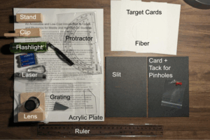
An example of a basic kit of materials used for all for the experiments.
In this one-day workshop for four educators, Dr. Keathley modeled a curriculum covering ray optics and waves, with hands-on experiments on imaging, fiber optics, and spectroscopy which involved low-cost and non-specialized materials. To the right is one of the experimental material kits given to the teachers. He taught them as if they were the students, handing out textbook-like material which included the how-to on the experiment. He also discussed how the curriculum could be used, including breaking points to simplify or extend the material.
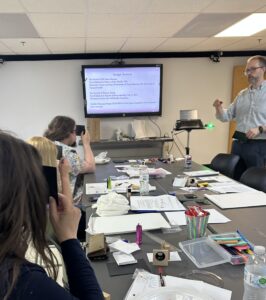
Teachers testing an experiment on the wave pattern of light using black index cards with two pin-holes while Dr. Keathley explains
As part of the proposal for his NSF CAREER award Dr. Keathley included an optics outreach effort in Eastern Kentucky. The NSF has a long-term interest in broadening the pool of future scientists. But as to why work with Eastern Kentucky in particular? The Appalachia region, including Eastern Kentucky, have historically low STEM engagement and opportunity. Additionally, when researching outreach efforts, Donnie found many more efforts targeting urban areas, and thus decided to take the opportunity to focus his outreach on more rural environments. He was able to connect with KVEC before submitting the proposal, and they were interested in working with him.
As a final draw to selecting this area, Dr. Keathley grew up in the region and recalls the relative sparsity of opportunities to engage with STEM compared to areas like the Boston metro area with large science museums, research universities, and STEM industry.
Throughout the year-long design process, KVEC’s input on community needs and connections to educators were crucial. While Dr. Keathley’s original idea focused on a hand-on optics workshop for the middle and high school students, KVEC’s experience helped reframe it to focus on teaching the teachers for a larger and more enduring impact. As Dr. Keathley notes, the impact of an outreach event can be “frustratingly nebulous and difficult to define rigorously.” However, by focusing on educators, the impact of one workshop can not only endure over multiple years but also touch hundreds of students. If each of the four teachers were able to incorporate even one new experiment and unit from the workshop, about 425 students would benefit in the first year alone. And the community outreach is not planned to end after this one event. KVEC and Donnie plan to follow up with these four teachers with a zoom call in December on how and if they have been able to incorporate it into their curriculum. Also, the initial planning for a second workshop next summer is already underway!
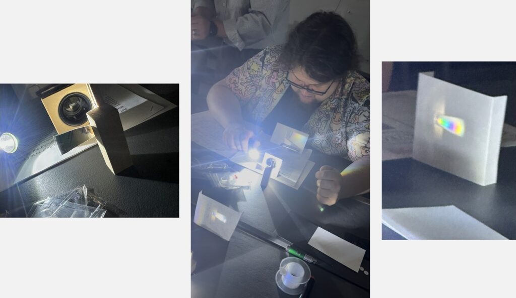
An educator at a workshop performing an experiment on making a camera image of a very clear example of a diffraction grating.
For additional photos from the event, visit KVEC’s flicker account.