News
New Publication “Compact and Tunable Forward Coupler Based on High-Impedance Superconducting Nanowires”
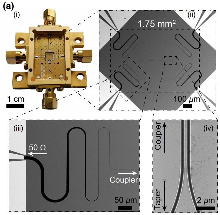
Developing compact, low-dissipation, cryogenic-compatible microwave electronics is essential for scaling up low-temperature quantum computing systems. In this paper, we demonstrate an ultracompact microwave directional forward coupler based on high-impedance slow-wave superconducting-nanowire transmission lines. The coupling section of the fabricated device has a footprint of 416μm2. At 4.753 GHz, the input signal couples equally to the through port and forward-coupling port (50:50) at −6.7dB with −13.5dB isolation. The coupling ratio can be controlled with dc bias current or temperature by exploiting the dependence of the kinetic inductance on these quantities. The material and fabrication processes are suitable for direct integration with superconducting circuits, providing a practical solution to the signal distribution bottlenecks in developing large-scale quantum computers.
A complete description of the work may be found here.
New Publication “Superconducting MoN thin films prepared by DC reactive magnetron sputtering for nanowire single-photon detectors”
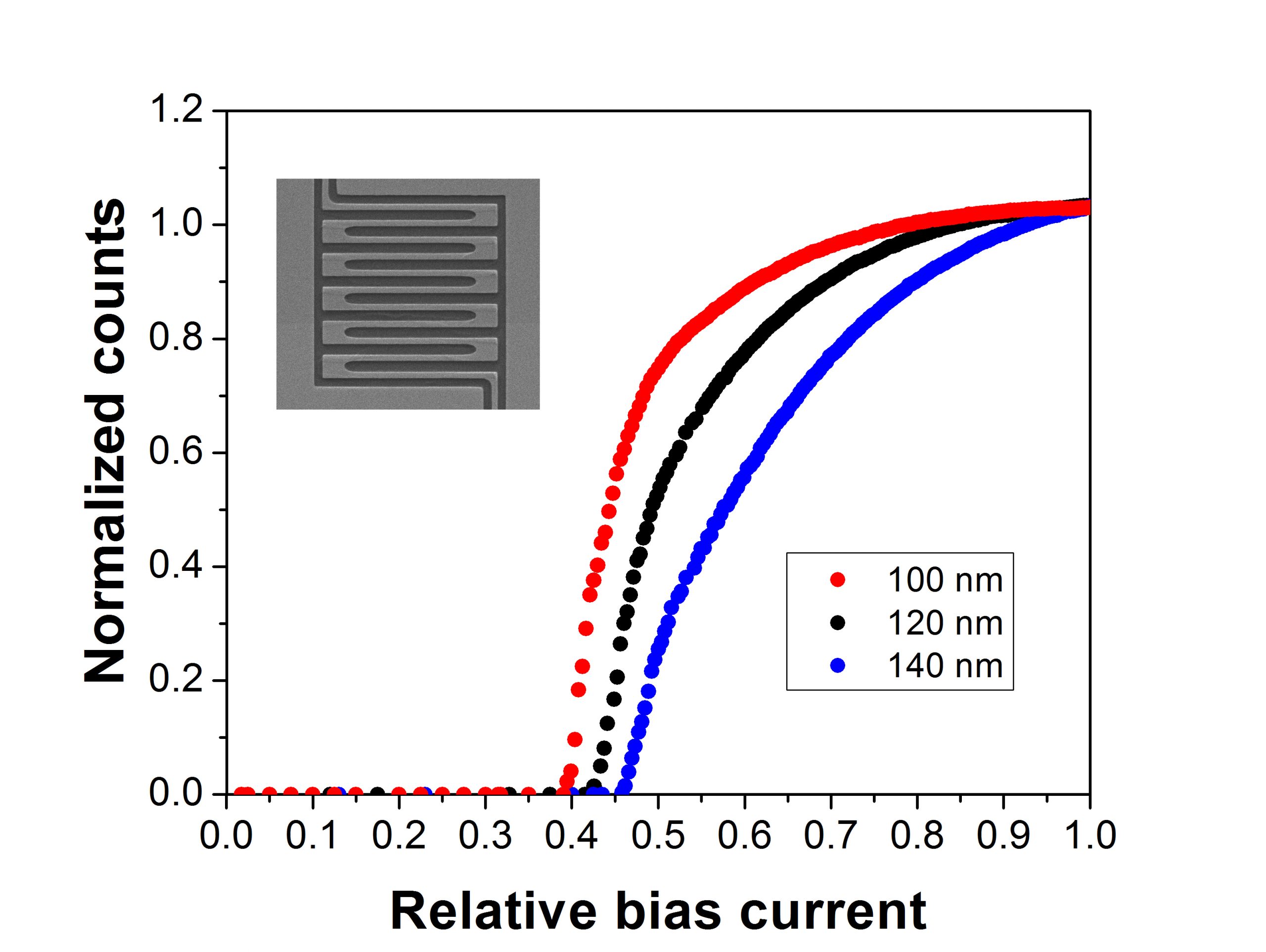
We present a comprehensive study of molybdenum nitride (MoN) thin film deposition using direct current reactive magnetron sputtering. We have investigated the effect of various deposition conditions on the superconducting and electrical properties of the films. Furthermore, we have shown that meander-shaped single-photon detectors made from 5 nm MoN films have
saturated quantum detection efficiency at the telecom wavelength of 1550 nm. Our results indicate that MoN may be a material of interest for practical applications of low-temperature superconductors, including single-photon detectors and transition-edge sensors.
A complete description of the work may be found here.
New Publication “Enhancing the performance of superconducting nanowire-based detectors with high-filling factor by using variable thickness ”
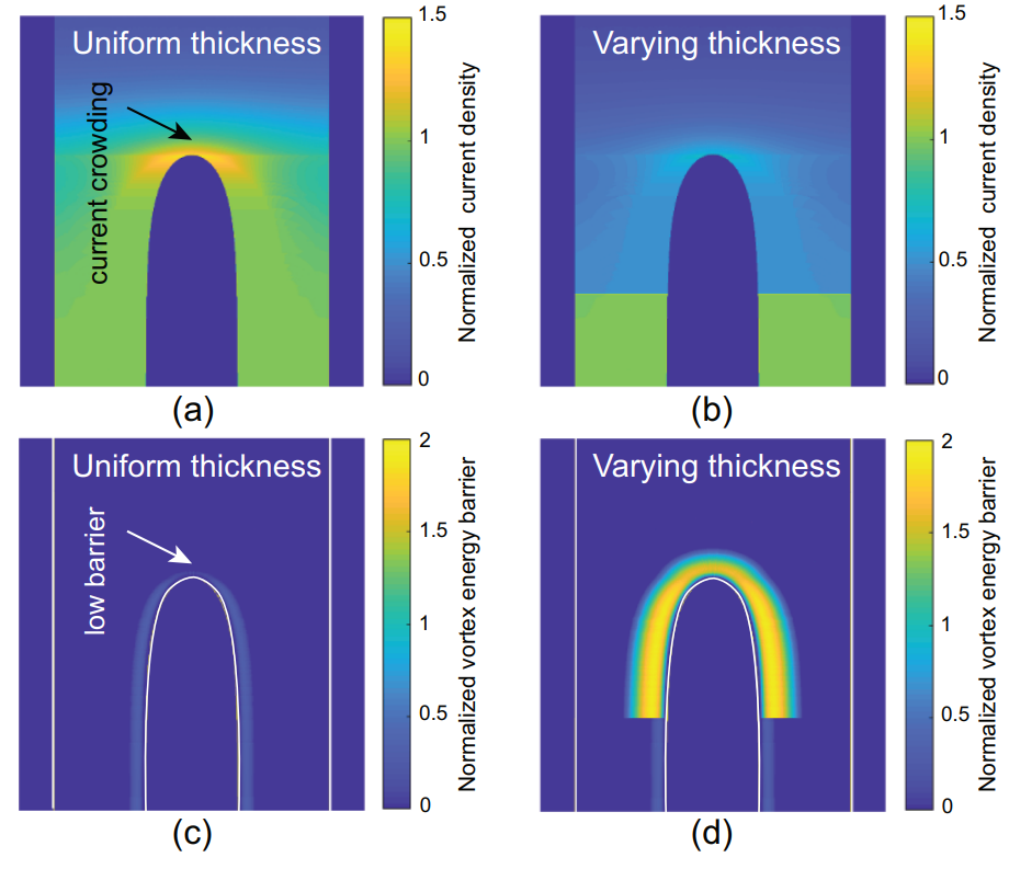
Current crowding at bends of superconducting nanowire single-photon detector (SNSPD) is one of the main factors limiting the performance of meander-style detectors with large filling factors. In this paper, we propose a new concept to reduce the influence of the current crowding effect, a so-called variable thickness SNSPD, which is composed of two regions with different thicknesses. A larger thickness of bends in comparison to the thickness of straight nanowire sections locally reduces the current density and reduces the suppression of the critical current caused by current crowding. This allows variable thickness SNSPD to have a higher critical current, an improved detection efficiency, and decreased dark count rate in comparison with a standard uniform thickness SNSPD with an identical geometry and film quality.
A complete description of the work may be found here.
New Publication “Superconducting Nanowire Spiking Element for Neural Networks ”
As the limits of traditional von Neumann computing come into view, the brain’s ability to communicate vast quantities of information using low-power spikes has become an increasing source of inspiration for alternative architectures. Key to the success of these largescale neural networks is a power-efficient spiking element that is scalable and easily interfaced with traditional control electronics. In this work, we present a spiking element fabricated from superconducting nanowires that has pulse energies on the order of ∼10 aJ. We demonstrate that the device reproduces essential characteristics of biological neurons, such as a refractory period and a firing threshold. Through simulations using experimentally measured device parameters, we show how nanowire-based networks may be used for inference in image recognition and that the probabilistic nature of nanowire switching may be exploited for modeling biological processes and for applications that rely on stochasticity.
A complete description of the work may be found here.
New Publication “Fabrication of gold nanostructures using wet lift-off without adhesion promotion”
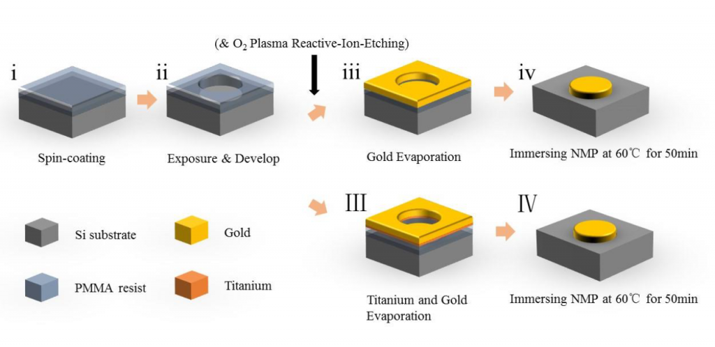
The use of an intervening adhesion layer is essential in reliable fabrication of noble metallic nanostructures for optical and electronic devices. However, many emerging applications such as plasmonics and transfer printing raise the demand of metallic structures without adhesion layers, either to mitigate the plasmon damping or to facilitate the transfer processes. In this work, we systematically investigate the fabrication reliability of adhesion-free lithographic gold nanostructures on Si wafers and gold-coated substrates using a wet lift-off process. According to a large amount of statistical results, we comprehensively evaluate the patterning behavior of metallic nanostructures without adhesion promotion. Analytical modelling and control experiments are carried out to characterize the mechanics of their failure behaviors as a function of morphology and surface property. Our work provides useful information to the nanofabrication community to obtain adhesion-free gold nanostructures for plasmonic and transfer printing applications.
A complete description of the work may be found here.