News
New Publication “Large-area microwire MoSi single-photon detectors at 1550 nm wavelength”
We demonstrate saturated internal detection efficiency at 1550 nm wavelengths for meander-shaped superconducting nanowire single-photon detectors made of 3 nm thick MoSi films with widths of 1 and 3 μm and active areas up to 400 × 400 μm2. Despite hairpin turns and a large number of squares (up to 104) in the device, the dark count rate was measured to be ∼103 cps at 99% of the switching current. This value is about two orders of magnitude lower than the results reported recently for short MoSi devices with shunt resistors. We also found that 5 nm thick MoSi detectors with the same geometry were insensitive to single near-infrared photons, which may be associated with different levels of suppression of the superconducting order parameter. However, our results obtained on 3 nm thick MoSi devices are in good agreement with predictions in the frame of a kinetic-equation approach
A complete description of the work may be found here.
Talks at CLEO Conference
Our group participated to the CLEO2020 conference with four talks. You can find the recordings at the following links:
- Dr. Mina Bionta Towards Integrated Attosecond Time-Domain Spectroscopy (00:02:05) [also featured in the talk: What’s Next in Ultrafast Optics – Hot Topics at CLEO: 2020]
- Marco Colangelo Superconducting nanowire single-photon detector on thin-film lithium niobate photonic waveguide (01:30:48) [also featured in the talk: What’s Next in Integrated Photonics – Hot Topics at CLEO: 2020]
- Marco Turchetti Low-Energy Optical Pulse Detection Using Biased Plasmonic Nanoantenna (00:02:33)
- Dr. Di Zhu – highlighted talk (30 min) – Photon-Number Resolution Using Superconducting Tapered Nanowire Detector (00:59:41)
New video “Optimizing Superconducting Thin Films for Nanowire Single Photon Detectors”
MIT Materials Research Laboratory 2019 Summer Scholar Leah Borgsmiller worked on niobium-aluminum thin films for superconducting nanowire single photon detectors in the QNN lab. Borgsmiller grew thin films, measured their superconducting transition temperature and optimized growth conditions
Optimizing Superconducting Thin Films for Nanowire Single Photon Detectors
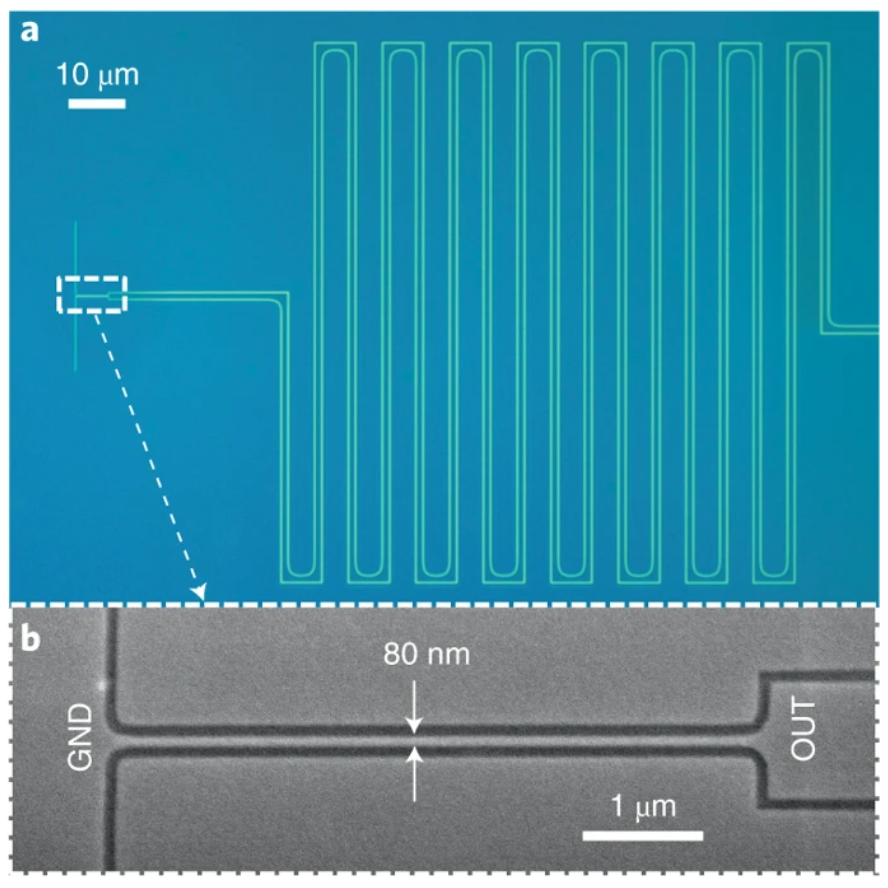
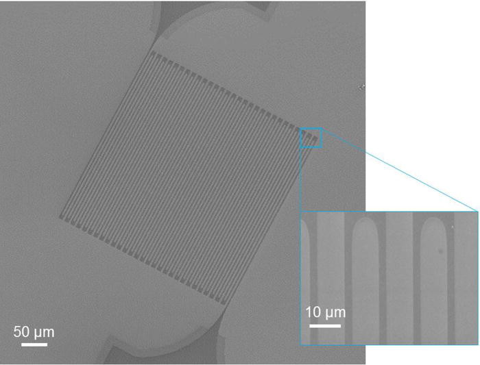
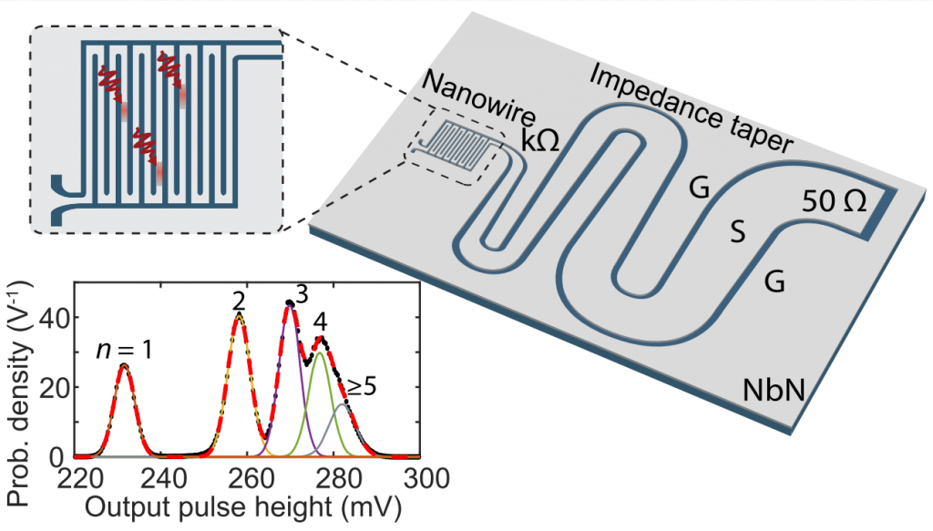
New Publication “Resolving photon numbers using a superconducting tapered nanowire detector”
Time- and number-resolved photon detection is crucial for quantum information processing. Existing photon-number-resolving (PNR) detectors usually suffer from limited timing and dark-count performance or require complex fabrication and operation. Here, we demonstrate a PNR detector at telecommunication wavelengths based on a single superconducting nanowire with an integrated impedance-matching taper. The taper provides a kΩ load impedance to the nanowire, making the detector’s output amplitude sensitive to the number of photon-induced hotspots. The prototyping device was able to resolve up to four absorbed photons with 16.1 ps timing jitter and <2 c.p.s. device dark count rate. Its exceptional distinction between single- and two-photon responses is ideal for high-fidelity coincidence counting and allowed us to directly observe bunching of photon pairs from a single output port of a Hong-Ou-Mandel interferometer. This detector architecture may provide a practical solution to applications that require high timing resolution and few-photon discrimination.
A complete description of the work may be found here.
New Publication “Demonstration of sub-3 ps temporal resolution with a superconducting nanowire single-photon detector”
Improvements in temporal resolution of single-photon detectors enable increased data rates and transmission distances for both classical and quantum optical communication systems, higher spatial resolution in laser ranging, and observation of shorter-lived fluorophores in biomedical imaging. In recent years, superconducting nanowire single-photon detectors (SNSPDs) have emerged as the most efficient time-resolving single-photon-counting detectors available in the near-infrared, but understanding of the fundamental limits of timing resolution in these devices has been limited due to a lack of investigations into the timescales involved in the detection process. We introduce an experimental technique to probe the detection latency in SNSPDs and show that the key to achieving low timing jitter is the use of materials with low latency. By using a specialized niobium nitride SNSPD we demonstrate that the system temporal resolution can be as good as 2.6 ± 0.2 ps for visible wavelengths and 4.3 ± 0.2 ps at 1,550 nm.
A complete description of the work may be found here.