News
New Grant “Nanostructured optical-field samplers for visible to near-infrared time-domain spectroscopy”
QNN awarded new SENSE.nano seed grant for the development of nanostructured optical-field samplers for visible to near-infrared time-domain spectroscopy.
More information on this project and the other SENSE.nano awards may be found here.
New Publication “Single-Photon Single-Flux Coupled Detectors”
In this work, we present a novel device that is a combination of a superconducting nanowire single-photon detector and a superconducting multilevel memory. We show that these devices can be used to count the number of detections through single-photon to single-flux conversion. Electrical characterization of the memory properties demonstrates single-flux quantum (SFQ) separated states. Optical measurements using attenuated laser pulses with different mean photon number, pulse energies and repetition rates are shown to differentiate single-photon detection from other possible phenomena, such as multiphoton detection and thermal activation. Finally, different geometries and material stacks to improve device performance, as well as arraying methods, are discussed.
A complete description of the work may be found here.
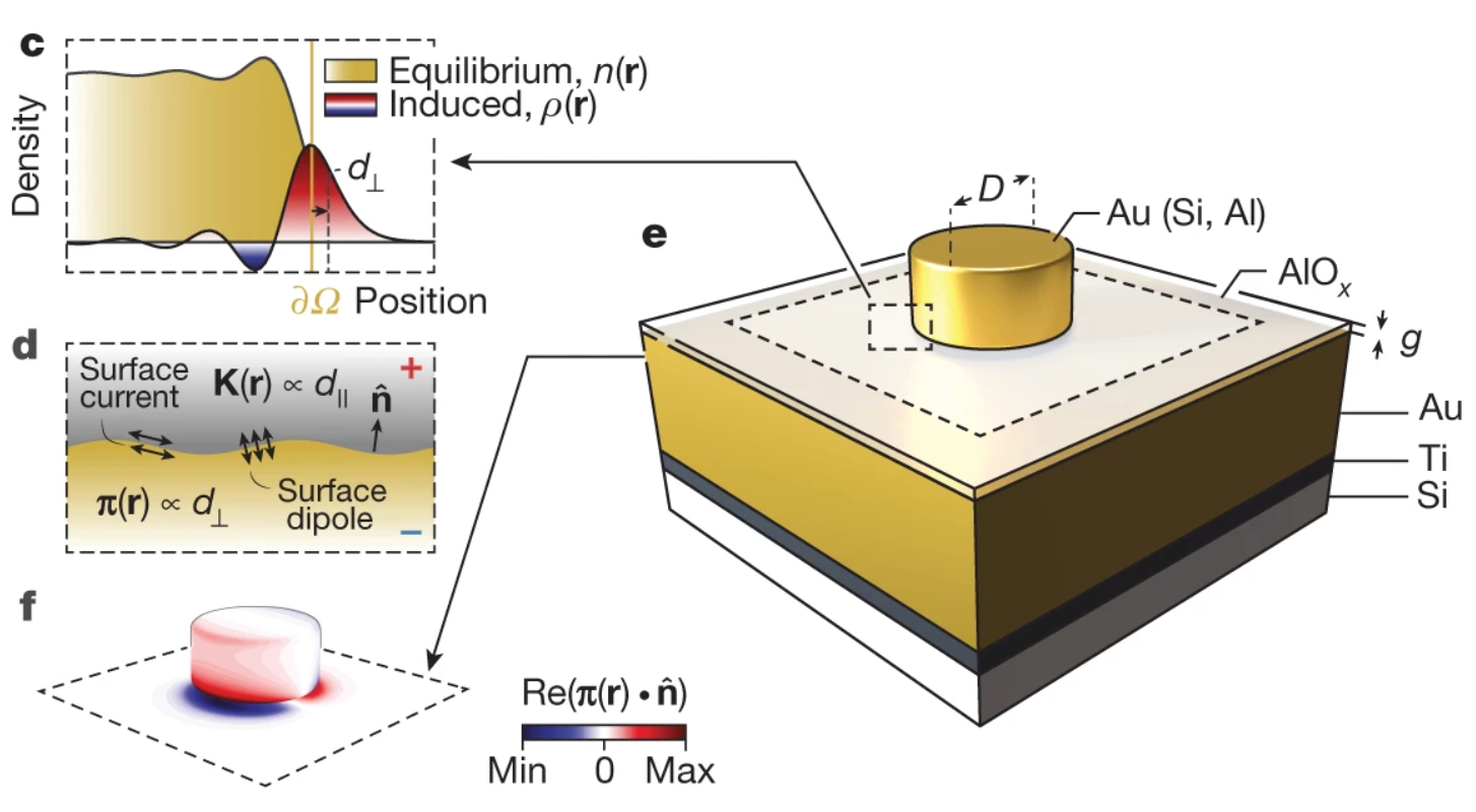
New Publication “A general theoretical and experimental framework for nanoscale electromagnetism”
The macroscopic electromagnetic boundary conditions, which have been established for over a century, are essential for the understanding of photonics at macroscopic length scales. Even state-of-the-art nanoplasmonic studies, exemplars of extremely interface-localized fields, rely on their validity. This classical description, however, neglects the intrinsic electronic length scales (of the order of ångström) associated with interfaces, leading to considerable discrepancies between classical predictions and experimental observations in systems with deeply nanoscale feature sizes, which are typically evident below about 10 to 20 nanometres. The onset of these discrepancies has a mesoscopic character: it lies between the granular microscopic (electronic-scale) and continuous macroscopic (wavelength-scale) domains. Existing top-down phenomenological approaches deal only with individual aspects of these omissions, such as nonlocality and local-response spill-out. Alternatively, bottom-up first-principles approaches—for example, time-dependent density functional theory are severely constrained by computational demands and thus become impractical for multiscale problems. Consequently, a general and unified framework for nanoscale electromagnetism remains absent. Here we introduce and experimentally demonstrate such a framework—amenable to both analytics and numerics, and applicable to multiscale problems—that reintroduces the electronic length scale via surface-response functions known as Feibelman d parameters. We establish an experimental procedure to measure these complex dispersive surface-response functions, using quasi-normal-mode perturbation theory and observations of pronounced nonclassical effects. We observe nonclassical spectral shifts in excess of 30 per cent and the breakdown of Kreibig-like broadening in a quintessential multiscale architecture: film-coupled nanoresonators, with feature sizes comparable to both the wavelength and the electronic length scale. Our results provide a general framework for modeling and understanding nanoscale (that is, all relevant length scales above about 1 nanometre) electromagnetic phenomena.
A complete description of the work may be found here.
Andrew Dane awarded Best Poster at the 706th W.E. Heraeus Seminar
Congratulations to Andrew Dane, who won the best poster award at the 706th W.E. Heraeus Seminar, titled Superconducting Kinetic Inductances for his work on high-Q superconducting niobium resonators incorporating nanoscale quasiparticle traps.
Details regarding his poster abstract may be found below:
Superconducting Nb Resonators with Gold Nanodot Decorations
Andrew Dane, Omid Noroozian, Emily Barrentine, Di Zhu, Thomas Stevenson, Harvey Moseley, Karl Berggren
While the operation of kinetic inductance detectors (KIDs) is well understood, reports of anomalous behaviors in KIDs fabricated from highly-disordered, thin-film superconductors indicate that a detailed understanding of the superconducting density of states and behavior of excited quasiparticles is necessary to reconcile experimental findings with theory. Anomalous behaviors include: (1) differences in the inductive and dissipative photo-response times, such that the shift in the frequency of the resonator outlasts the reduction in Q by a factor of four, (2) resonant frequency vs temperature that cannot be explained by Mattis-Bardeen theory without ad-hoc modifications. It has been observed experimentally that in highly-disordered thin-film superconductors, spontaneous fluctuations of the superconducting gap can arise. The interaction between excited quasiparticles and a spatially varying gap may explain the anomalous behaviors observed in KIDs, for instance if quasiparticle trap states exist that can temporarily localize excited quasiparticles.
In this work, we report on the fabrication and measurement of Nb CPW resonators, as well as progress towards a physical simulation of the case where the superconducting gap varies along the resonator body. The Nb used for fabrication was 50 nm thick, sputtered onto r-plane sapphire at 500 °C, and was not expected to have significant variation in the gap along the film. In order to produce a spatially varying gap, we lithographically defined arrays of gold nano-dots, on top of the CPW centerline, in an attempt to locally reduce the superconducting gap in the Nb due to the proximity effect. In undecorated resonators at high photon number, an internal Q of greater than one million was measured at 7 mK, while the internal Q of the decorated resonators was substantially less. The resonant behavior of these devices vs temperature and power, and their relevance to high-kinetic inductance materials will be discussed.

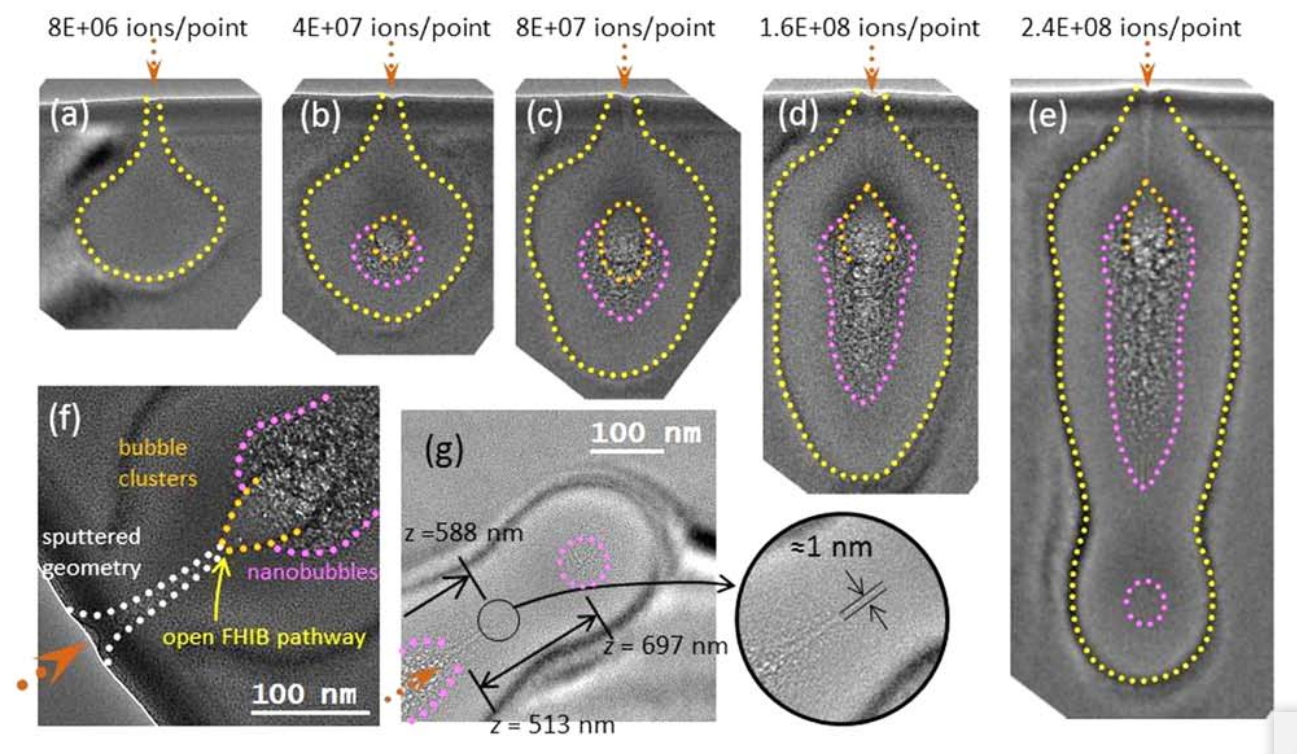
New Publication “Focused-helium-ion-beam blow forming of nanostructures: radiation damage and nanofabrication”
Targeted irradiation of nanostructures by a finely focused ion beam provides routes to improved control of material modification and understanding of the physics of interactions between ion beams and nanomaterials. Here, we studied radiation damage in crystalline diamond and silicon nanostructures using a focused helium ion beam, with the former exhibiting extremely long-range ion propagation and large plastic deformation in a process visibly analogous to blow forming. We report the dependence of damage morphology on material, geometry, and irradiation conditions (ion dose, ion energy, ion species, and location). We anticipate that our method and findings will not only improve the understanding of radiation damage in isolated nanostructures, but will also support the design of new engineering materials and devices for current and future applications in nanotechnology.
A complete description of the work may be found here.