News
Emily Toomey awarded 3rd prize in the “Schnitzer Prize in the Visual Arts” contest
Congratulations to Emily for being awarded the 3rd prize in the “Schnitzer Prize in the Visual Arts” contest.
Established in 1996, the Harold and Arlene Schnitzer Prize is awarded each year to current MIT undergraduate and graduate students for excellence in a body of work. Students submit their artistic portfolios for consideration. The 2019 Schnitzer Prize winners attest to the broad range of visual artistic expression that thrives at MIT.

Emily Toomey selected as 2019 AAAS Mass Media Fellow
Congratulations to Emily Toomey for being selected as 2019 AAAS Mass Media Fellow.
The AAAS Mass Media Fellowship is a competitive program aimed at encouraging communication in science and fostering connections between scientists and journalists. Each year, fellows are placed at media organizations nationwide for ten weeks to write and report on the latest news in science, and to explain scientific concepts to a broad audience. This year, 26 fellows were selected based on resumes, writing samples, and recommendations. Emily will be working at Smithsonian Magazine in Washington, D.C.

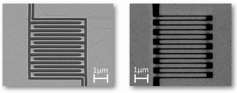
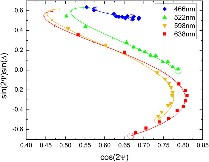
New Publication “Measuring thickness in thin NbN films for superconducting devices”
The authors present the use of a commercially available fixed-angle multiwavelength ellipsometer for quickly measuring the thickness of NbN thin films for the fabrication and performance improvement of superconducting nanowire single photon detectors. The process can determine the optical constants of absorbing thin films, removing the need for inaccurate approximations. The tool can be used to observe oxidation growth and allows thickness measurements to be integrated into the characterization of various fabrication processes.
A complete description of the work may be found here.
John Simonaitis awarded NSF fellowship
Congratulations to John Simonaitis on receiving the National Science Foundation Graduate Research Fellowship. This prestigious and competitive award will support his work for three years.
![]()
New Publication “Enhancement of Optical Response in Nanowires by Negative-Tone PMMA Lithography”
The method of negative-tone polymethyl methacrylate (PMMA) electron-beam lithography is investigated to improve the performance of nanowire-based superconducting detectors. Using this approach, the superconducting nanowire single-photon detectors (SNSPDs) have been fabricated from 5-nm-thick NbN film sputtered at room temperature. To investigate the impact of this process, SNSPDs were prepared by positive-tone- and negative-tone-PMMA lithography, and their electrical and photodetection characteristics at 4.2 K were compared. The SNSPDs made by negative-tone-PMMA lithography show higher critical-current density and higher photon count rate at various wavelengths. Our results suggest a higher negative-tone-PMMA technology may be preferable to the standard positive-tone-PMMA lithography for this application.
A complete description of the work may be found here.