News
New video “Studying Superconducting Thin Films”
Summer Program: Studying superconducting thin film
This summer, Lily Hallett investigated superconducting MoN thin films for use in nanowire single-photon detectors. She optimized deposition conditions for DC Magnetron Sputtering of MoN films and studied their superconducting and electrical properties. Low-pressure annealing experiments were performed in the sputtering chamber to increase the critical temperature of 5 nm films.
Studying Superconducting Thin Films
New Publication “Frequency Pulling and Mixing of Relaxation Oscillations in Superconducting Nanowires”
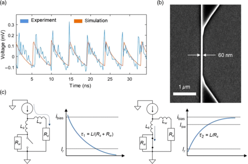
Many superconducting technologies such as rapid single-flux quantum computing and superconducting quantum-interference devices rely on the modulation of nonlinear dynamics in Josephson junctions for functionality. More recently, however, superconducting devices have been developed based on the switching and thermal heating of nanowires for use in fields such as single-photon detection and digital logic. In this paper, we use resistive shunting to control the nonlinear heating of a superconducting nanowire and compare the resulting dynamics to those observed in Josephson junctions. We show that interaction of the hotspot-impedance with an external shunt produces high-frequency relaxation oscillations with similar behavior to that observed in Josephson junctions due to their ability to be modulated by a weak periodic signal. In particular, we use a microwave drive to pull and mix the oscillation frequency, resulting in phase-locked features that resemble the Shapiro steps observed in the ac Josephson effect. Microwave nanowire devices based on these conclusions have promising applications in fields such as parametric amplification and frequency mixing.
A complete description of the work may be found here.
Citation:
Emily Toomey, Qing-Yuan Zhao, Adam N. McCaughan, Karl K. Berggren. “Frequency pulling and mixing of relaxation oscillations in superconducting nanowires” Physical Review Applied 9, 6 (2018)
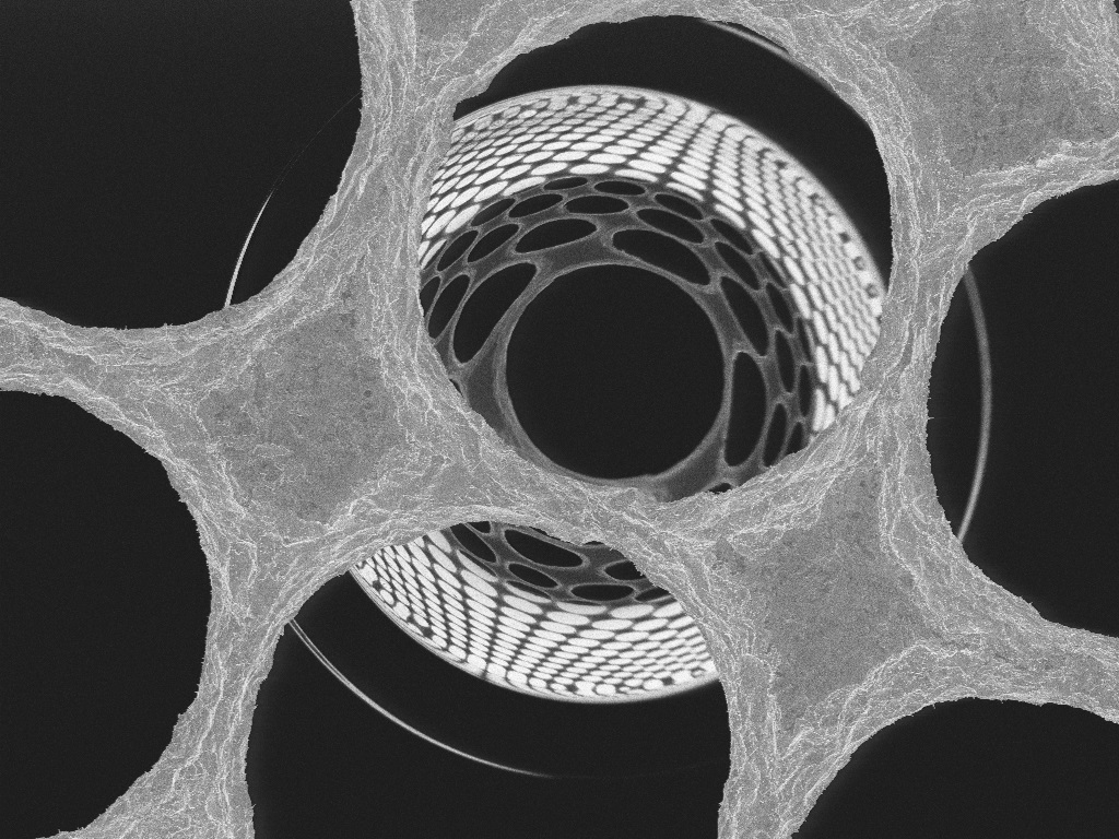
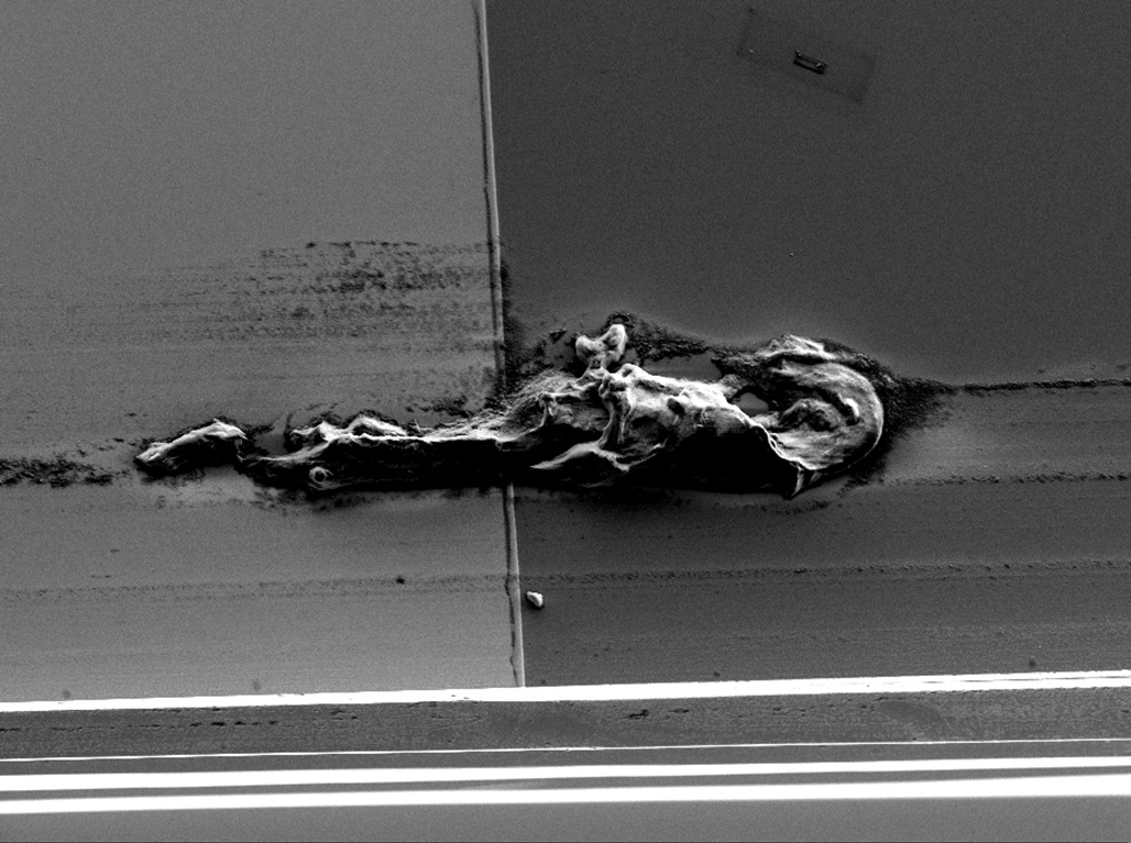
Navid Abedzadeh awarded Best Electron Beam and Emily Toomey, Marco Colangelo and Navid Abedzadeh got an honorable mention at EIPBN Micrograph Contest 2018
Congratulations to Navid Abedzadeh for being awarded Best Electron Beam and congratulations to Emily Toomey, Marco Colangelo and Navid Abedzadeh for the honorable mention in the Micrograph Contest at this year’s EIPBN conference in Puerto Rico. All the competing micrographs can be found here.
View Navid’s winning micrograph “Black hole in an SEM”
View Emily, Marco and Navid electron micrograph “Why did the chicken cross the wafer?”
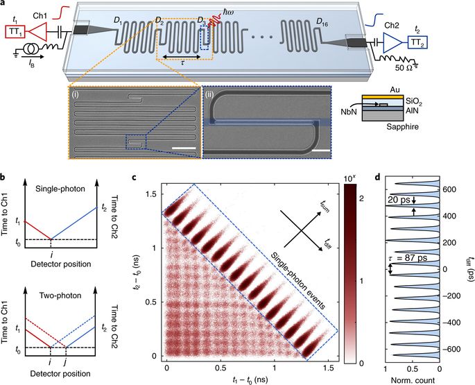
New Publication “A scalable multi-photon coincidence detector based on superconducting nanowires”
Coincidence detection of single photons is crucial in numerous quantum technologies and usually requires multiple time-resolved single-photon detectors. However, the electronic readout becomes a major challenge when the measurement basis scales to large numbers of spatial modes. Here, we address this problem by introducing a two-terminal coincidence detector that enables scalable readout of an array of detector segments based on superconducting nanowire microstrip transmission line. Exploiting timing logic, we demonstrate a sixteen-element detector that resolves all 136 possible single-photon and two-photon coincidence events. We further explore the pulse shapes of the detector output and resolve up to four-photon events in a four-element device, giving the detector photon-number-resolving capability. This new detector architecture and operating scheme will be particularly useful for multi-photon coincidence detection in large-scale photonic integrated circuits.
A complete description of the work may be found here.
Citation:
Di Zhu, Qing-Yuan Zhao, Hyeongrak Choi, Tsung-Ju Lu, Andrew E. Dane, Dirk R. Englund, Karl K. Berggren. “A scalable multi-photon coincidence detector based on superconducting nanowires” Nature Nanotechnology (2018)
New Publication “Exploring proximity effects and large depth of field in helium ion beam lithography: large-area dense patterns and tilted surface exposure”
Helium ion beam lithography (HIL) is an emerging nanofabrication technique. It benefits from a reduced interaction volume compared to that of an electron beam of similar energy, and hence reduced long-range scattering (proximity effect), higher resist sensitivity and potentially higher resolution. Furthermore, the small angular spread of the helium ion beam gives rise to a large depth of field. This should enable patterning on tilted and curved surfaces without the need of any additional adjustments, such as laser-auto focus. So far, most work on HIL has been focused on exploiting the reduced proximity effect to reach single-digit nanometer resolution, and has thus been concentrated on single-pixel exposures over small areas. Here we explore two new areas of application. Firstly, we investigate the proximity effect in large-area exposures and demonstrate HIL’s capabilities in fabricating precise high-density gratings on large planar surfaces (100 μm × 100 μm, with pitch down to 35 nm) using an area dose for exposure. Secondly, we exploit the large depth of field by making the first HIL patterns on tilted surfaces (sample stage tilted 45°). We demonstrate a depth of field greater than 100 μm for a resolution of about 20 nm.
A complete description of the work may be found here.
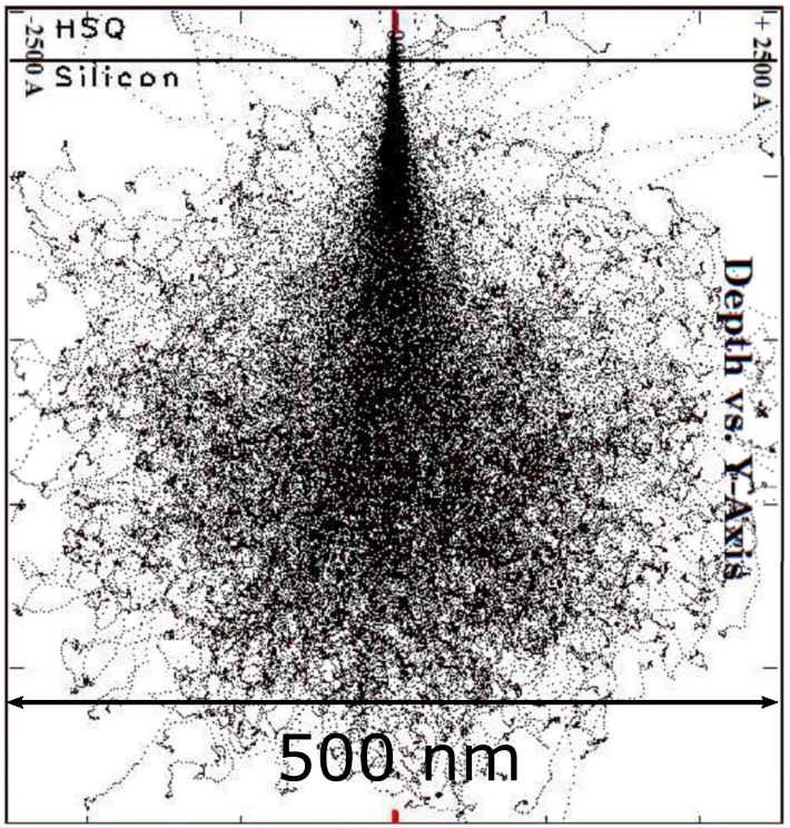
Citation:
Ranveig Flatabø, Akshay Agarwal, Richard Hobbs, Martin M Greve, Bodil Holst and Karl K Berggren “Exploring proximity effects and large depth of field in helium ion beam lithography: large-area dense patterns and tilted surface exposure” Nanotechnology 29, 27 (2018)