News
Marco Turchetti awarded Best Invited Poster at EIPBN
Congratulations to Marco Turchetti for being awarded Best Invited Poster at this year’s EIPBN conference in Orlando, FL. Details regarding his poster abstract may be found below:
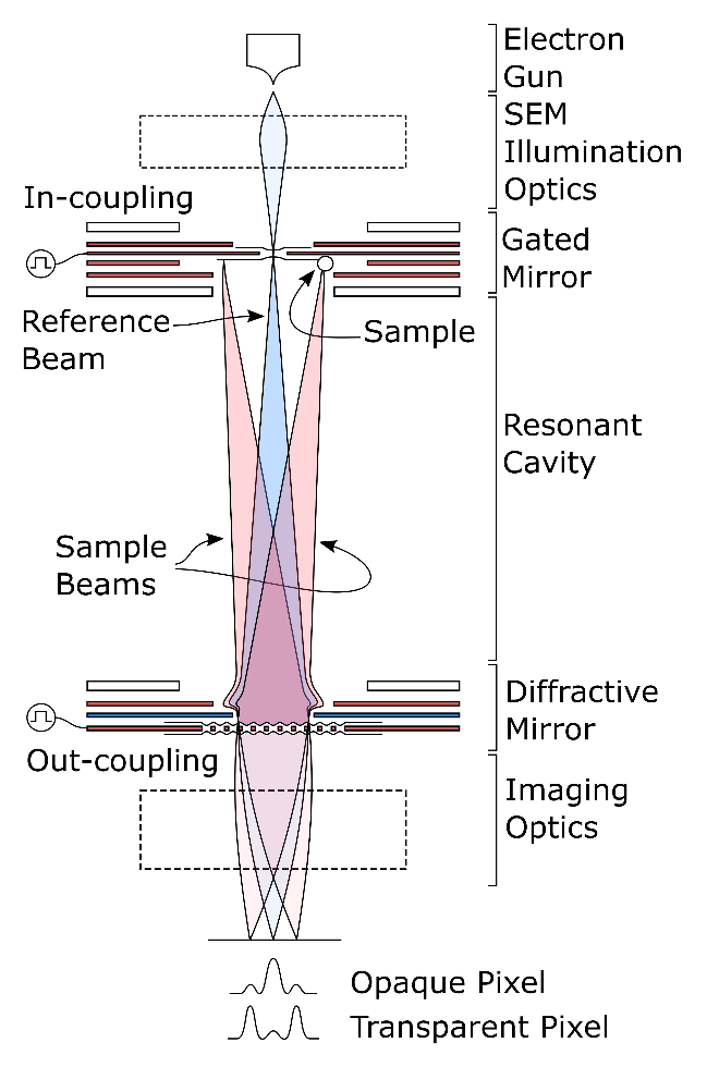
Aberration-Corrected Quantum Electron Microscopy
Marco Turchetti, Chung-Soo Kim, Richard Hobbs, Navid Abedzadeh, Pieter Kruit and Karl K. Berggren
Quantum electron microscopy (QEM) is one of the most promising approaches that could overcome the resolution limit imposed by the radiation damage due to the minimum electron dose necessary to surpass shot noise. This is recognized as the main resolution limit when imaging biological specimens. A QEM scheme exploits the concept of interaction-free measurement in a resonant electron optical cavity, whose purpose is to generate and sustain two coupled states of the electron wavefunction, the reference and the sample states. In this work, we designed and simulated a linear resonant electron cavity, the core of a QEM apparatus, and we analysed the properties of each components necessary to build such a cavity. Moreover, we proposed and simulated two possible modifications to the base scheme demonstrating that they could efficiently be employed to correct spherical aberration inside the cavity. This could significantly improve the system final resolution. One involves insertion of a quadrupole-octupole corrector inside the cavity. The second one, instead involves substitution of the gated mirror with a hyperbolic triode mirror.
New publication: “A nanofabricated, monolithic, path-separated electron interferometer”
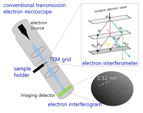
We describe a modular, self-aligned, amplitude-division electron interferometer in a conventional transmission electron microscope. The interferometer consists of two 45-nm-thick silicon layers separated by 20 μm. This interferometer is fabricated from a single-crystal silicon cantilever on a transmission electron microscope grid by gallium focused-ion-beam milling. Using this interferometer, we obtain interference fringes in a Mach-Zehnder geometry in an unmodified 200 kV transmission electron microscope. The fringes have a period of 0.32 nm, which corresponds to the [1̄1̄1] lattice planes of silicon, and a maximum contrast of 15%. We use convergent-beam electron diffraction to quantify grating alignment and coherence. This design can potentially be scaled to millimeter-scale, and used in electron holography. It could also be applied to perform fundamental physics experiments, such as interaction-free measurement with electrons. A complete description of the work may be found here.
Citation:
Akshay Agarwal, Chung-Soo Kim, Richard Hobbs, Dirk van Dyck and Karl K. Berggren. “A nanofabricated, monolithic, path-separated electron interferometer,” Scientific Reports, 7, 1677 (2017) . DOI: 10.1038/s41598-017-01466-0
Navid Abedzadeh awarded NSERC Fellowship
New publication: “Single-photon imager based on a superconducting nanowire delay line”
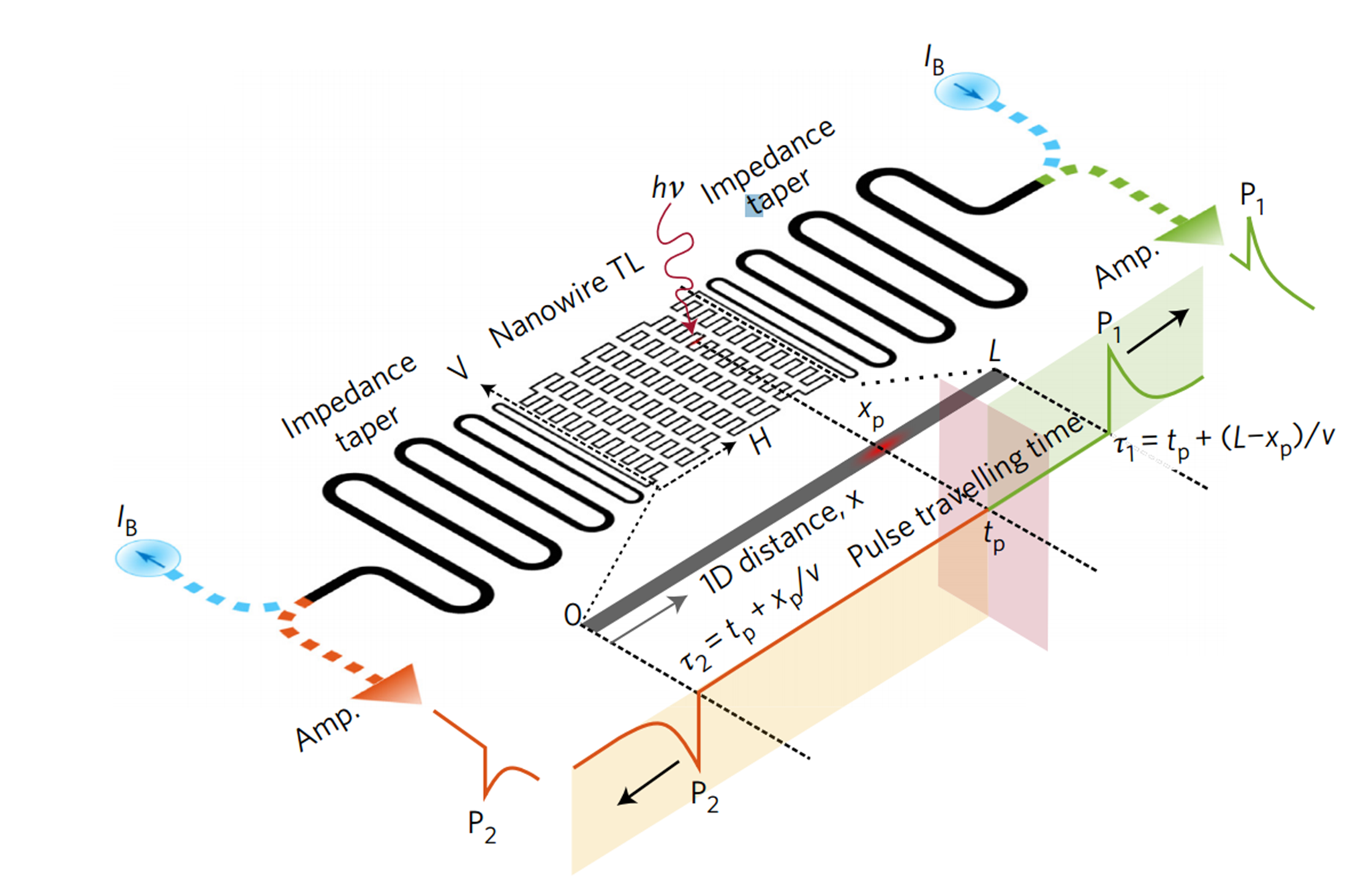
 We demonstrate a scalable single-photon imager using a single continuous superconducting nanowire that is not only a single-photon detector but also functions as an efficient microwave delay line. In this context, photon-detection pulses are guided in the nanowire and enable the readout of the position and time of photon-absorption events from the arrival times of the detection pulses at the nanowire’s two ends. Experimentally, we slowed down the velocity of pulse propagation to ∼2% of the speed of light in free space. In a 19.7 mm long nanowire that meandered across an area of 286 × 193 μm2, we were able to resolve ∼590 effective pixels with a temporal resolution of 50 ps (full width at half maximum). The nanowire imager presents a scalable approach for high-resolution photon imaging in space and time. A full description of the publication may be found here.
Citation:
Qing-Yuan Zhao , Di Zhu, Niccolò Calandri, Andrew E. Dane , Adam N. McCaughan, Francesco Bellei, Hao-Zhu Wang, Daniel F. Santavicca, and Karl K. Berggren. “Single-photon imager based on a superconducting nanowire delay line,” Nature Photonics, vol. 11, p247-252, 2017.
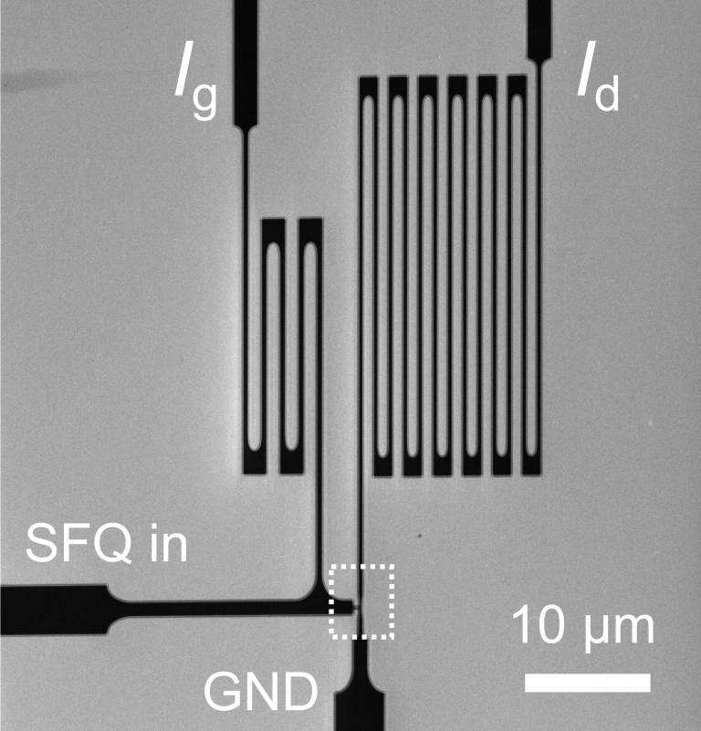
New publication: “A nanocryotron comparator can connect single-flux-quantum circuits to conventional electronics”
We demonstrate the use of a single three-terminal superconducting-nanowire device, called the nanocryotron (nTron), as a digital comparator to combine SFQ circuits with mature semiconductor circuits such as complementary metal oxide semiconductor (CMOS) circuits. Since SFQ circuits can digitize output signals from general superconducting devices and CMOS circuits can interface existing CMOS-compatible electronics, our results demonstrate the feasibility of a general architecture that uses an nTron as an interface to realize a ‘super-hybrid’ system consisting of superconducting detectors, superconducting quantum electronics, CMOS logic gates and memories, and other conventional electronics. A full description of the publication may be found here.
Citation:
Qing-Yuan Zhao, Adam N. McCaughan, Andrew E. Dane, Karl K. Berggren, Thomas Ortlepp.“A nanocryotron comparator can connect single-flux-quantum circuits to conventional electronics,” Supercond. Sci. Technol., vol. 30, no. 4, p. 044002, 2017.