News
New Patent on Self-Assembly Issued to QNN Group Members
A method developed by the QNN Group with collaborators promises a way to make complex two-dimensional patterns by using sparse lithography in combination with self-assembly. Such a technique could be useful for nanofabrication of integrated-circuit patterns, or patterns for solar cells, meta-materials, or other applications where complex two-dimensional nano-designs are needed. Congratulations to the authors JB Chang, Hong-Kyoon Choi, Adam Hannon, Caroline Ross, and Karl Berggren.
A copy of the patent can be found here.
New paper: “Control of zinc oxide nanowire array properties with electron-beam lithography templating for photovoltaic applications” accepted to Nanotechnology
[abstract] We found that electron-beam lithography, a top-down approach, is a suitable prototyping method for templating and controlling hydrothermally-grown ZnO nanowires (NWs). By varying the deposition method of the ZnO seed layer, annealing and template hole diameter, the branching and alignment parameters of the NW growth was determined. We uncovered the relationship between mutual impingement and template hole size, as well as found ideal growth parameters for well-aligned, single NWs. These results can allow for higher efficiency in ZnO NW-based solar cells.
nanotechweb.org highlighted this article in February 2015. It was also featured in the nanotechweb.org spring round-up.
The paper by Samuel M. Nicaise, Jayce J. Cheng, Amirreza Kiani, Silvija Gradečak, and Karl K. Berggren has been accepted to Nanotechnology and is currently open access here.
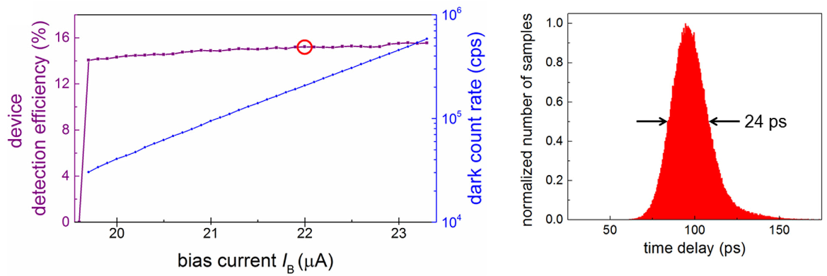
24-picosecond single-photon timing jitter in saturated SNSPDs – New Paper in IEEE Quantum Electronics
In our new paper, to appear in the IEEE Jornal of Selected Topics in Quantum Electronics (JSTQE), we have demonstrated fully-saturated nanowire single-photon detectors with 24 ps jitter. Furthermore we show an improved fabrication process that allowed us to increase the fabrication yield of our detectors.
The JSTQE preprint is available at doi:10.1109/JSTQE.2014.2372054
http://ieeexplore.ieee.org/
New paper: “Universal scaling of the critical temperature for thin films near the superconducting-to-insulating transition” accepted to Phys. Rev. B
[preprint] [supp. info.] We reported that the superconducting properties scale universally close to the superconducting-to-insulating transition in thin films. This universal behavior was found useful not only for the fundamental understanding of superconductivity near its onset, but also for miniaturized superconducting devices, such as superconducting-nanowire single-photon detectors.
MIT News highlighted this article in December 2014.
The paper by Yachin Ivry, Chung-Soo Kim, Andrew E. Dane, Domenico De Fazio, Adam McCaughan, Kristen A. Sunter, Qingyuan Zhao and Karl K. Berggren has been accepted to Phys. Rev B and is currently on the arXiv and in abstract.
New paper: “High-Yield, Ultrafast, Plasmon-Enhanced Au Nanorod Optical Field Emitter Arrays” accepted to ACS Nano
Here we demonstrate the design, fabrication and characterization of ultrafast, surface-plasmon enhanced Au nanorod optical field emitter arrays. We present a quantitative study of electron emission from Au nanorod arrays fabricated by high-resolution electron beam lithography and excited by 35 fs pulses of 800 nm light. We present accurate models for both the optical field enhancement of Au nanorods within high-density arrays, and electron emission from those nanorods. We have also studied the effects of surface plasmon damping induced by metallic interface layers at the substrate/nanorod interface on near-field enhancement and electron emission. We have identified the peak optical field at which the electron emission mechanism transitions from a 3-photon absorption mechanism to strong-field tunneling emission. Moreover, we have investigated the effects of nanorod array density on nanorod charge yield, including measurement of space-charge effects. The Au nanorod photocathodes presented in this work display 100-1000 times higher conversion efficiency relative to previously reported UV triggered emission from planar Au photocathodes. Consequently, the Au nanorod arrays triggered by ultrafast pulses of 800 nm light in this work, may outperform equivalent UV-triggered Au photocathodes, while also offering nanostructuring of the electron pulse produced from such a cathode, which is of interest for x-ray free-electron laser (XFEL) development where nanostructured electron pulses may facilitate more efficient and brighter XFEL radiation.
The paper by Richard G Hobbs, Yujia Yang, Arya Fallahi, Phillip D. Keathley, Eva De Leo, Franz X. Kärtner, William S. Graves, and Karl K. Berggren has been accepted to ACS Nano.