News
Matthew Yeung awarded the Mathworks Fellowship

Matthew Yeung is a PhD candidate whose research explores interactions between light and nanostructures for both fundamental research and the development of novel optoelectronic technologies. The focus of his current work, which will be supported by this MathWorks Fellowship, is the development of nanostructured devices that can interact with and measure light fields with sub-femtosecond resolution. These devices enable a critical new tool in visible to near-infrared optical metrology: a sampling oscilloscope for light waves, which could offer a fresh time-domain perspective on how light interacts with materials. Matthew’s work has large number of potential applications, including the creation of more efficient solar cells, understanding the fundamental energy transfer mechanisms that enable photosynthesis, and characterizing materials with unprecedented sensitivity. MATLAB has been vital in Matthew’s device design, experiment development, and instrumentation interfacing, and he looks forward to sharing the resulting tools with the MathWorks community. His work has the potential to help usher in revolutionary advances in light-based technologies.
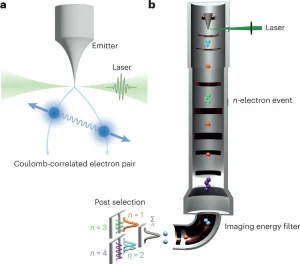
New Publication: “Twin experiments reveal twin electron dynamics”
Dr. Donnie Keathley and John Simonaitis reviewed a double-submission of papers on using coulombic effects for electron heralding for Nature Physics, and were invited to write a News and Views article for the general public. The complete article can be found here.
Abstract:
Two studies of electrons generated from laser-triggered emitters have found highly predictable electron–electron energy correlations. These studies, at vastly different energy scales, may lead to heralded electron sources, enabling quantum free-electron optics and low-noise, low-damage electron beam lithography and microscopy.

A schematic of the two experiments, showing the underlying mechanism and detection schemes.
Thesis Defense Recording – Dr. Marco Colengelo: Superconducting Nanowire Technology For Microwave and Photonics Applications

Now-Dr. Marco Colangelo’s thesis defense is now available to view online. The title is “Superconducting Nanowire Technology For Microwave and Photonics Applications.” Congratulations for Dr. Colangelo for his successful PhD defense!
Abstract:
Quantum computing and quantum communication are innovative technologies that promise to revolutionize several aspects of our societal landscape. However, early cutting-edge experiments are rapidly approaching significant scalability roadblocks. As the qubit count increases, superconducting quantum processors require an increasing number of control and readout electronic devices, which are incompatible at scale with the performance of dilution refrigerators. Photonic-based platforms struggle with integration issues due to operational, design, and heterogeneous material compatibility. In this talk, I will demonstrate that superconducting nanowires have the potential to drive a major leap in the scalability of these and other architectures. I will show that the exotic microwave properties of superconducting nanowires enable cryogenic devices at microwave frequencies with an ultra-compact footprint. I will introduce microwave directional couplers and resonators featuring a footprint reduction of up to 200 times, making them suitable for on-chip integration with superconducting quantum processors and any application needing cryogenic microwave signal processing. Furthermore, I will show that engineering the nanowire properties can overcome the metrics trade-offs of single-photon detectors. I will demonstrate an all-in-one nanowire detector with record performances, imaging capabilities, and photon-number resolution capabilities, all in the same design. This device can be used to scale experiments needing many high-performance detectors. Finally, I will demonstrate single-photon detectors integrated on lithium-niobate-on-insulator with state-of-the-art performance. I will also introduce integrated array technology on silicon-on-insulator. This nanowire technology can be heterogeneously integrated with current quantum photonic platforms on-chip, removing the need for outcoupling to fiber-coupled detectors. Superconducting nanowires have the potential to become a comprehensive solution for scaling classical and quantum architectures.
Committee: Prof Karl Berggren (Thesis Supervisor), Prof. Dirk Englund, and Prof. Daniel Santavicca
[embedyt] https://www.youtube.com/watch?v=afFOGF2CMAA[/embedyt]
Webinar: Nanoscale Petahertz Electronics for Science and Technology
 Dr. Donnie Keathley will be presenting at an open webinar on May 5th at 1pm EDT. The topic will be “Nanoscale Petahertz Electronics for Science and Technology.” Details for the webinar are on the registration website and below.
When matter is driven by intense, few-cycle optical field waveforms it is possible to generate free-electrons having sub-cycle, sub-femtosecond temporal structure. By driving such emission between nanoscale structures, it is possible to create compact optical-field-driven electronic devices having bandwidths approaching or even exceeding one petahertz (10^15 hertz).
In this webinar, Phillip Keathley will start by reviewing the fundamental principles behind strong-field electron emission and how it enables sub-femtosecond electron emission. From there, Dr. Keathley will review recent efforts using these properties of strong-field electron emisison for the development of chip-scale petahertz electronics. In particular, Dr. Keathley will review his team’s efforts using nanoplasmonics to enable the use of low-energy driving pulses (picojoule- to nanojoule-level) for applications such as shot-to-shot carrier-envelope-phase detection and optical field sampling with attosecond resolution. Dr. Keathley will conclude by discussing how these nanoscale devices are enabling new capabilities. These new capabilities include field-resolved optical detection as well as the ability to transfer information between devices over femtosecond timescales for petahertz-level memory and logic gates.
Subject Matter Level: Intermediate – Assumes basic knowledge of the topic
What You Will Learn:
• Fundamentals of strong-field electron emission
• How strong-field electron emission enables field-resolved detection and petahertz-electronics
• A review of the state of the art in the field
• Future directions for these technologies
Who Should Attend:
• Those interested in ultrafast optics and applications
• Scientists working in strong-field light-matter interactions
• Those working in nanotechnology interested in how they could be used for ultrafast optics applications
• Those interested in optoelectronics and new directions for ultrafast optical detection
QNN Quarterly Newsletter
 Welcome to another QNN Newsletter! We have had a couple departures and some arrivals, as well as some exciting papers come out. Karl spent a few days with students at Jefferson lab in Virginia and at Fermilab in the Chicago area, working on interacting with the high-energy physics community, where there is some interest in the superconducting nanowires for electronics in their detectors. We also were happy to host a visit by Prof. Billy Putnam from UCDavis, our collaborator on both a DOE and NSF program related to free electrons coupled to nano-optical systems.
Best regards,
Karl and Donnie
Comings and Goings
The last few months we’ve welcomed the following new group members:
- Valentin Karem, Visiting Student
- Sahil Pontula, UROP
The following members have now left and become alumni group members:
- Shruti Nirantar, now a visiting scientist at the NASA Ames Research Center
- Torque El Dandachi, now working at Microsoft as a Quantum Simulation Engineer
Theses!
T. El Dandachi, “Efficient simulation of Large-Scale Superconducting Nanowire Circuits,” M.Eng. Thesis, Massachusetts Institute of Technology, 2023.
A. Bechhofer, “Geometrical Optimization of Planar Nano Vacuum Channel Transistors,” M.S. Thesis, Massachusetts Institute of Technology, 2023.
Publications (11/1/22 – 02-28-23)
A. Buzzi, M. Castellani, R. A. Foster, O. Medeiros, M. Colangelo, and K. K. Berggren, “A Nanocryotron Memory and Logic Family.” arXiv, Dec. 15, 2022. doi: 10.48550/arXiv.2212.07953.
R. A. Foster, M. Castellani, A. Buzzi, O. Medeiros, M. Colangelo, and K. K. Berggren, “A Superconducting Nanowire Binary Shift Register.” arXiv, Feb. 09, 2023. Accessed: Feb. 17, 2023. [Online]. Available: http://arxiv.org/abs/2302.04942
S. I. Davis et al., “Improved Heralded Single-Photon Source with a Photon-Number-Resolving Superconducting Nanowire Detector,” Phys. Rev. Applied, vol. 18, no. 6, p. 064007, Dec. 2022, doi: 10.1103/PhysRevApplied.18.064007.
Y. Hochberg et al., “New constraints on dark matter from superconducting nanowires,” Phys. Rev. D, vol. 106, no. 11, p. 112005, Dec. 2022, doi: 10.1103/PhysRevD.106.112005.
E. Batson et al., “Reduced ITO for Transparent Superconducting Electronics.” arXiv, Dec. 16, 2022. doi: 10.48550/arXiv.2212.08573.
E. Piatti et al., “Reversible Tuning of Superconductivity in Ion-Gated NbN Ultrathin Films by Self-Encapsulation with a High-k Dielectric Layer,” Phys. Rev. Applied, vol. 18, no. 5, p. 054023, Nov. 2022, doi: 10.1103/PhysRevApplied.18.054023.
P. D. Keathley, S. V. B. Jensen, M. Yeung, M. R. Bionta, and L. B. Madsen, “Uncovering extreme nonlinear dynamics in solids through time-domain field analysis,” Phys. Rev. B, vol. 107, no. 5, p. 054302, Feb. 2023, doi: 10.1103/PhysRevB.107.054302.
Talks (11-01-22 to 02-28-23)
K. K. Berggren, “The Cryotron Reborn: Superconducting-Nanostrip-Based Electronics,” presented at the Applications of Superconducting Electronics and Detectors Workshop, Newport News, VA, Nov. 30, 2022.

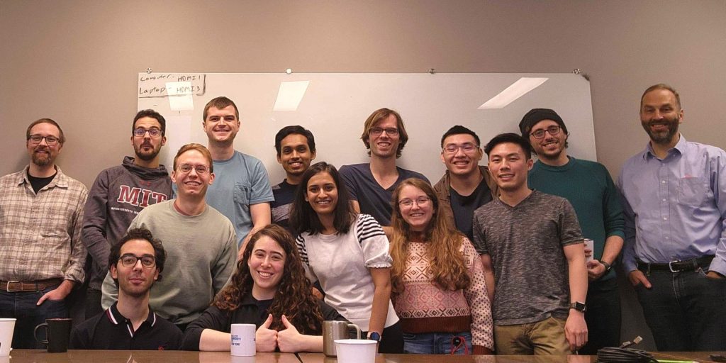
Shruti’s farewell get together on January 6th. From right to left: Karl Berggren, Stewart Koppel, Matthew Yeung, Lu-Ting Chou, Emma Batson, Maurice Krieelart, Shruti Nirantar, DJ Paul, Adina Bechhofer, Owen Medeiros, John Simonaitis, Marco Colangelo, Torque El Dandachi, and Donnie Keathley.