News
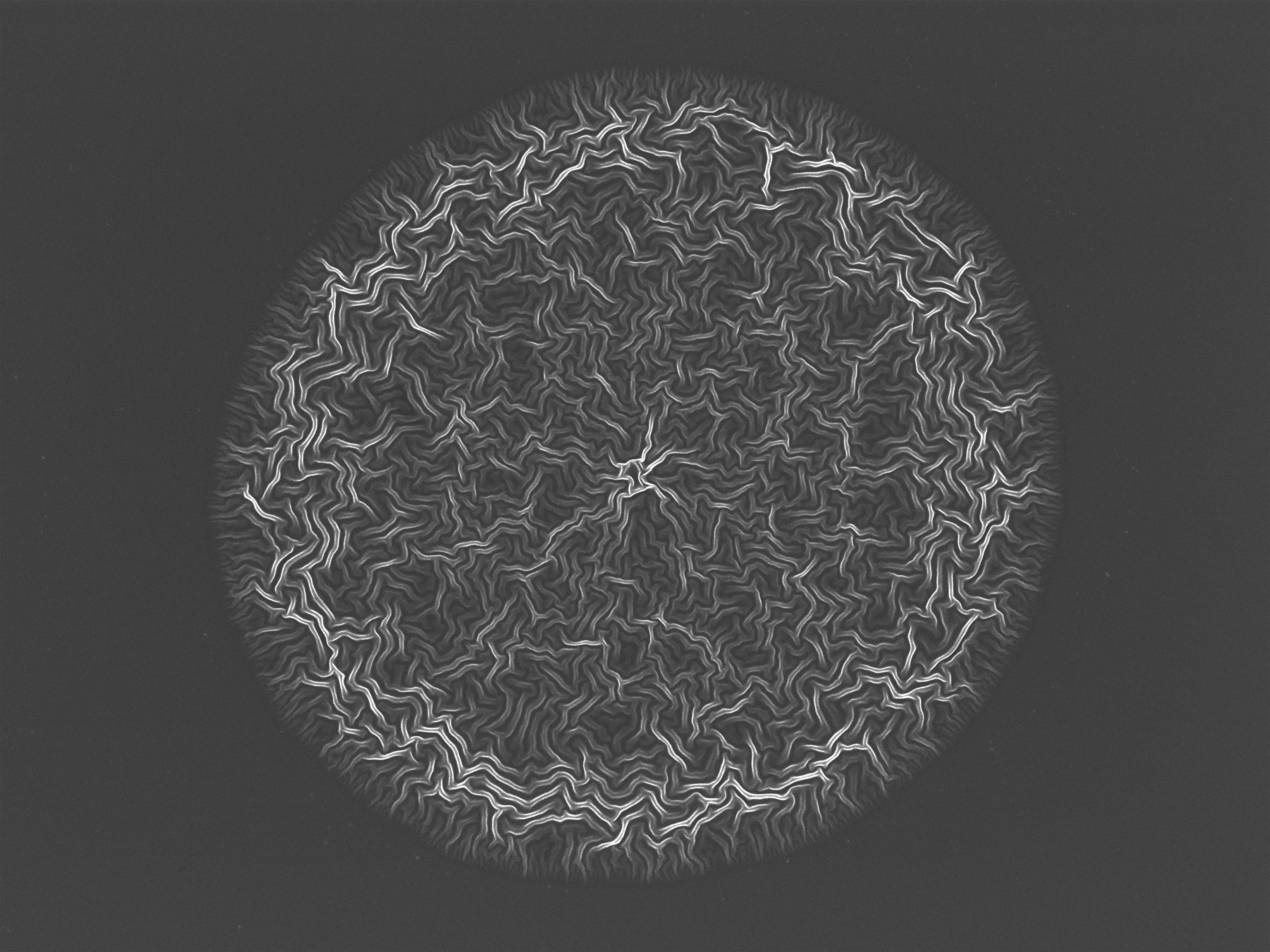
EIPBN 2022 Best Electron Micrograph Award
Congratulations to Alessandro Buzzi and Matteo Castellani for winning the award for the “Best Electron Micrograph” for their image entitled “A Maze in Grace.”
New Publication “Electron Emission Regimes of Planar Nano Vacuum Emitters”
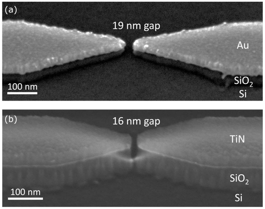
Recent advancements in nanofabrication have enabled the creation of vacuum electronic devices with nanoscale free-space gaps. These nanoelectronic devices promise the benefits of cold-field emission and transport through free space, such as high nonlinearity and relative insensitivity to temperature and ionizing radiation, all while drastically reducing the footprint, increasing the operating bandwidth, and reducing the power consumption of each device. Furthermore, planarized vacuum nanoelectronics could easily be integrated at scale similar to typical microscale and nanoscale semiconductor electronics. However, the interplay between different electron emission mechanisms from these devices is not well understood, and inconsistencies with pure Fowler-Nordheim (FN) emission have been noted by others. In this work, we systematically study the current-voltage characteristics of planar vacuum nanodevices having few-nanometer radii of curvature and free-space gaps between the emitter and the collector. By investigating the current-voltage characteristics of nearly identical devices fabricated from two different materials and under various environmental conditions, such as temperature and atmospheric pressure, we are able to clearly isolate three distinct emission regimes within a single device: Schottky, FN, and saturation. Our work will enable robust and accurate modeling of vacuum nanoelectronics, which will be critical for future applications requiring high-speed and low-power electronics capable of operation in extreme conditions.
A complete description of the work may be found here.
Honorable Mention in Poster Contest for Dip Joti Paul
Dip Joti Paul won an Honorable Mention in the DLS student poster contest held at CLEO in San Jose from May 7-12 for his poster “Infrared Refractive Index Measurement of Niobium Nitride Thin-Film via FTIR”.
See the full poster here.
New Publication “PHz Electronic Device Design and Simulation for Waveguide-Integrated Carrier-Envelope Phase Detection”
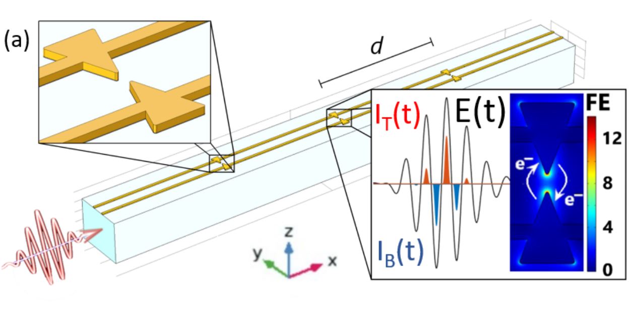
Carrier-envelope phase (CEP) detection of ultrashort optical pulses and low-energy waveform field sampling have recently been demonstrated using direct time-domain methods that exploit optical-field photoemission from plasmonic nanoantennas. These devices are compact and integratable solid-state detectors operating at optical frequencies under ambient conditions using low pulse energies (picojoule-level). Potential applications include frequency-comb stabilization, optical time-domain spectroscopy, compact tools for attosecond science and metrology, and petahertz-scale information processing. However, to date these devices have been driven by free-space optical waveforms and their implementation within integrated photonic platforms has yet to be demonstrated. In this work, we design and simulate fully-integrated plasmonic nanoantennas coupled to a SiN-core waveguide for CEP detection. We find that when coupled to realistic on-chip, few-cycle supercontinuum sources, these devices are suitable for direct time-domain CEP detection within integrated photonic platforms. We estimate a signal-to-noise ratio of 30 dB at 50 kHz resolution bandwidth, and address technical details, such as the tuning of the nanoantennas plasmonic resonance, CEP slippage in the waveguide, optical losses, and sensitivity to driving pulse characteristics such as energy and duration. Our results provide the basis for future design and fabrication of time-domain CEP detectors and allow for the development of fully-integrated attosecond science applications, frequency-comb stabilization and light-wave-based PHz electronics.
A complete description of the work may be found here.
QNN Quarterly Newsletter
We’ve had a busy summer in the lab and in terms of sharing our results. Here are a number of published papers and key activities.
Comings and Goings
This summer we welcomed the following new group members:
- Kate Artyunova, UROP
- Matteo Castellani, EECS Grad Student
- Andrew Sorenson, MEng Grad Student
The following members have now left and become alumni group members:
- Akshay Agarwal, completed his PhD!
- Thesis title “Techniques for Enhancing Electron Microscopy”
- Tao Cai, Summer UROP returning to University of Michigan
- Dario Cattozzo Mor, Junior Researcher at Czech Academy of Sciences
- Andres Lombo, returning to Senior year at University of Toronto
- Glenn Martinez, Successfully defended his MS Thesis!
- Di Zhu, taking technical staff position at IMRE in Singapore
Awards
- Marco Colangelo – Claude E. Shannon Award
Publications
[1] X. Zhang et al., “Physical properties of amorphous molybdenum silicide films for single-photon detectors,” Supercond. Sci. Technol., vol. 34, no. 9, p. 095003, Aug. 2021, doi:10.1088/1361-6668/ac1524.
[2] Q. Xie et al., “NbN-Gated GaN Transistor Technology for Applications in Quantum Computing Systems,” in 2021 Symposium on VLSI Technology, Jun. 2021, pp. 1–2.
[3] J. W. Simonaitis, B. Slayton, Y. Yang-Keathley, P. D. Keathley, and K. K. Berggren, “Precise, subnanosecond, and high-voltage switching enabled by gallium nitride electronics integrated into complex loads,” Review of Scientific Instruments, vol. 92, no. 7, p. 074704, Jul. 2021, doi:10.1063/5.0046706.
[4] D. Buckley, Y. Yang, Y. Yang-Keathley, K. K. Berggren, and P. D. Keathley, “Nanoantenna design for enhanced carrier–envelope-phase sensitivity,” J. Opt. Soc. Am. B, JOSAB, vol. 38, no. 9, pp. C11–C21, Sep. 2021, doi:10.1364/JOSAB.424549.
[5] M. R. Bionta et al., “On-chip sampling of optical fields with attosecond resolution,” Nat. Photonics, vol. 15, no. 6, pp. 456–460, Jun. 2021, doi:10.1038/s41566-021-00792-0.
[6] M. R. Bionta et al., “Tracking ultrafast solid-state dynamics using high harmonic spectroscopy,” Phys. Rev. Research, vol. 3, no. 2, p. 023250, Jun. 2021, doi:10.1103/PhysRevResearch.3.023250.
[7] R. Bhattacharya, M. Turchetti, P. D. Keathley, K. K. Berggren, and J. Browning, “Long term field emission current stability characterization of planar field emitter devices,” Journal of Vacuum Science & Technology B, vol. 39, no. 5, p. 053201, Sep. 2021, doi:10.1116/6.0001182.
[8] N. Abedzadeh et al., “Electrostatic electron mirror in SEM for simultaneous imaging of top and bottom surfaces of a sample,” Ultramicroscopy, vol. 226, p. 113304, Jul. 2021, doi:10.1016/j.ultramic.2021.113304.
Talks
CLEO2021
M. Colangelo et al., “Impedance-matched differential SNSPDs for practical photon counting with sub-10 ps timing jitter,” in Conference on Lasers and Electro-Optics (2021), May 2021, p. FW2P.1. doi:10.1364/CLEO_QELS.2021.FW2P.1.
M. Cattozzo Mor et al., “PHz Electronic Device Design for Waveguide-Integrated Carrier-Envelope Phase Detection,” in Conference on Lasers and Electro-Optics (2021), paper SW3J.3, May 2021, p. SW3J.3. doi:10.1364/CLEO_SI.2021.SW3J.3.
Lund Attosecond Symposium 2021
M. R. Bionta, “Tracking solid-state phase transitions with time-resolved HHG spectroscopy,” presented at the Lund Attoscience Symposium 2021, Virtual, Jun. 16, 2021.
IVNC2021
M. Turchetti, “Emission Behavior of Planar Nano-Vacuum Field Emitters,” presented at the 34th International Vacuum Nanoelectronics Conference, Virtual, Jul. 07, 2021. [Online].
LTD19
T. X. Zhou, “Ultra-wide MoSi SNSPD detectors,” presented at the 19th International Workshop on Low Temperature Detectors (LTD19), Virtual, Jul. 29, 2021. [Online].
ICN+T
P. D. Keathley, “On-Chip Petahertz Processing of Optical Fields,” presented at the ICN+T, Virtual, Jul. 2021.
Patents
Submission: US 63/076,463 Marco Turchetti, Mina R. Bionta, Felix Ritzkowsky, , Yujia Yang, Dario Cattozzo Mor, William P. Putnam, Franz X. Kärtner, Karl K. Berggren, Phillip D. Keathley “Integrated Optical Field Sampling Platform”