News
New Publication “Physical properties of amorphous molybdenum silicide films for single-photon detectors”
We systematically investigated the physical properties of amorphous MoxSi1−x films deposited by magnetron co-sputtering. The critical temperature Tc of MoxSi1−x films increases gradually with the Mo stoichiometry x, and the highest Tc = 7.9 K was found in Mo0.83Si0.17, where homogeneous films with the maximum Mo content can be obtained. The thick films of Mo0.83Si0.17 show surprising degradation in which the onset of zero-resistivity is suppressed below 2 K. The thin Mo0.83Si0.17films, however, reveal robust superconductivity even with thickness d ≈ 2 nm. We also characterized wide microwires based on the 2 nm thin Mo0.8Si0.2 films with wire widths 40 and 60 μm, which show single-photon sensitivity at 780 nm and 1550 nm wavelength.
A complete description of the work may be found here.
Talks at CLEO2021 Conference
Our group participated in the CLEO2021 conference with two talks. You can find the abstracts at the following links:
- Marco Colangelo – Impedance-matched differential SNSPDs for practical photon counting with sub-10 ps timing jitter
- Dario Cattozzo Mor – PHz Electronic Device Design for Waveguide-Integrated Carrier-Envelope Phase Detection
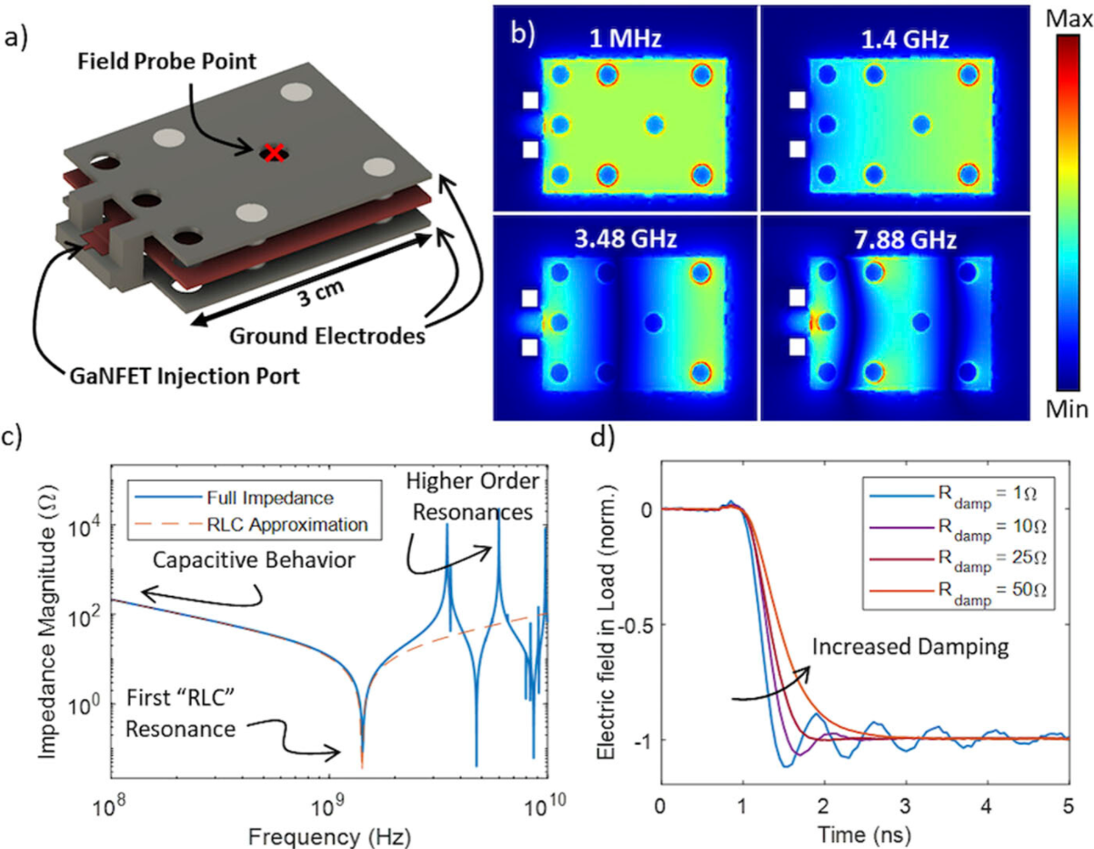
New Publication “Precise, subnanosecond, and high-voltage switching enabled by gallium nitride electronics integrated into complex loads”
In this work, we report the use of commercial gallium nitride (GaN) power electronics to precisely switch complex distributed loads, such as electron lenses and deflectors. This was accomplished by taking advantage of the small form-factor, low-power dissipation, and high temperature compatibility of GaN field effect transistors (GaNFETs) to integrate pulsers directly into the loads to be switched, even under vacuum. This integration reduces parasitics to allow for faster switching and removes the requirement to impedance match the load to a transmission line by allowing for a lumped element approximation of the load even with subnanosecond switching. Depending on the chosen GaNFET and driver, these GaN pulsers are capable of generating pulses ranging from 100 to 650 V and 5 to 60 A in 0.25–8 ns using simple designs with easy control, few-nanosecond propagation delays, and MHz repetition rates. We experimentally demonstrate a simple 250 ps, 100 V pulser measured by using a directly coupled 2 GHz oscilloscope. By introducing resistive dampening, we can eliminate ringing to allow for precise 100 V transitions that complete a −10 to −90 V transition in 1.5 ns, limited primarily by the inductance of the oscilloscope measurement path. The performance of the pulser attached to various load structures is simulated, demonstrating the possibility of even faster switching of internal fields in these loads. We test these circuits under vacuum and up to 120 °C to demonstrate their flexibility. We expect these GaN pulsers to have broad application in fields such as optics, nuclear sciences, charged particle optics, and atomic physics that require nanosecond, high-voltage transitions.
A complete description of the work may be found here.
Marco Colangelo named 2021 Claude E. Shannon Award Winner
Congratulations to Marco Colangelo on receiving the Claude E. Shannon Award. This prestigious and competitive award will support his work for one year.

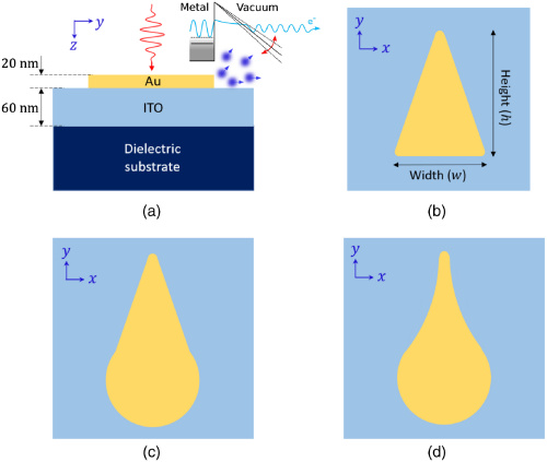
New Publication “Nanoantenna design for enhanced carrier–envelope-phase sensitivity”
Optical-field emission from nanostructured solids such as subwavelength nanoantennas can be leveraged to create sub-femtosecond, petahertz-scale electronics for optical-field detection. One application of particular interest is the detection of an incident optical pulse’s carrier–envelope phase (CEP). Such CEP detection requires few-cycle, broadband optical excitation where the resonant properties of the nanoantenna can strongly alter the response of the near field in time. Little quantitative investigation has been performed to understand how the geometry and resonant properties of the antennas should be tuned to enhance the CEP sensitivity and signal-to-noise ratio. Here we examine how the geometry and resonance frequency of planar plasmonic nanoantennas can be engineered to enhance the emitted CEP-sensitive photocurrent when driven by a few-cycle optical pulse. We find that with the simple addition of curved sidewalls leading to the apex, and proper tuning of the resonance wavelength, the net CEP-sensitive current per nanoantenna can be improved by 5−10×, and the signal-to-noise-ratio by 50−100× relative to simple triangular antennas operated on resonance. Our findings will inform the next generation of nanoantenna designs for emerging applications in ultrafast photoelectron metrology and petahertz electronics.
A complete description of the work may be found here.