Jun 19, 2015 | News Articles
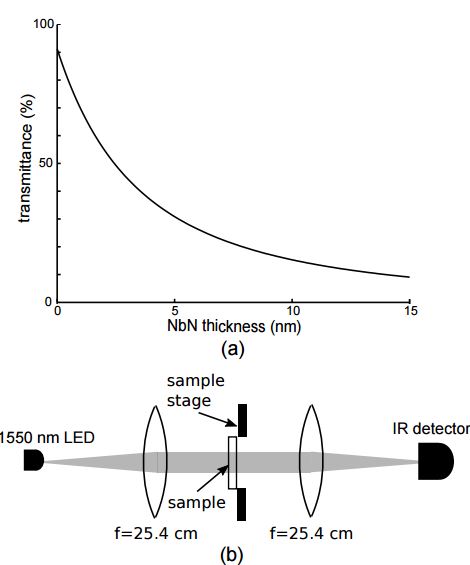
We built a transmissometer to determine the thickness of thin films of NbN that are deposited as the starting material for SNSPDs. The transmissometer measures the transmittance of light through NbN thin films, and the thickness of the NbN is found by fitting the...
Apr 29, 2015 | News Articles
Karl Berggren recently served as a member of MIT’s recent committee tasked with studying the nation’s “Innovation Deficit.” The outcome of the committee was a report in which a number of cases were studied, each of which illustrated...
Mar 26, 2013 | News Articles
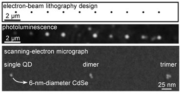
Nanotechweb has released a Journal Highlight of some of our recently published work. The research involves using electron beam lithography to precisely place quantum dots on a sample surface. The work explores size and height of different templating holes in a PMMA...