Jun 21, 2017 | News Articles, Uncategorized
Congratulations to Marco Turchetti for being awarded Best Invited Poster at this year’s EIPBN conference in Orlando, FL. Details regarding his poster abstract may be found below: Aberration-Corrected Quantum Electron Microscopy Marco Turchetti, Chung-Soo Kim,...
May 23, 2017 | News Articles, Uncategorized
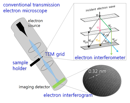
We describe a modular, self-aligned, amplitude-division electron interferometer in a conventional transmission electron microscope. The interferometer consists of two 45-nm-thick silicon layers separated by 20 μm. This interferometer is fabricated from a...
Apr 14, 2017 | News Articles
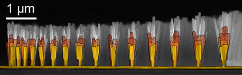
We demonstrate a scalable single-photon imager using a single continuous superconducting nanowire that is not only a single-photon detector but also functions as an efficient microwave delay line. In this context, photon-detection pulses are guided in the nanowire and...
Mar 8, 2017 | News Articles, Uncategorized
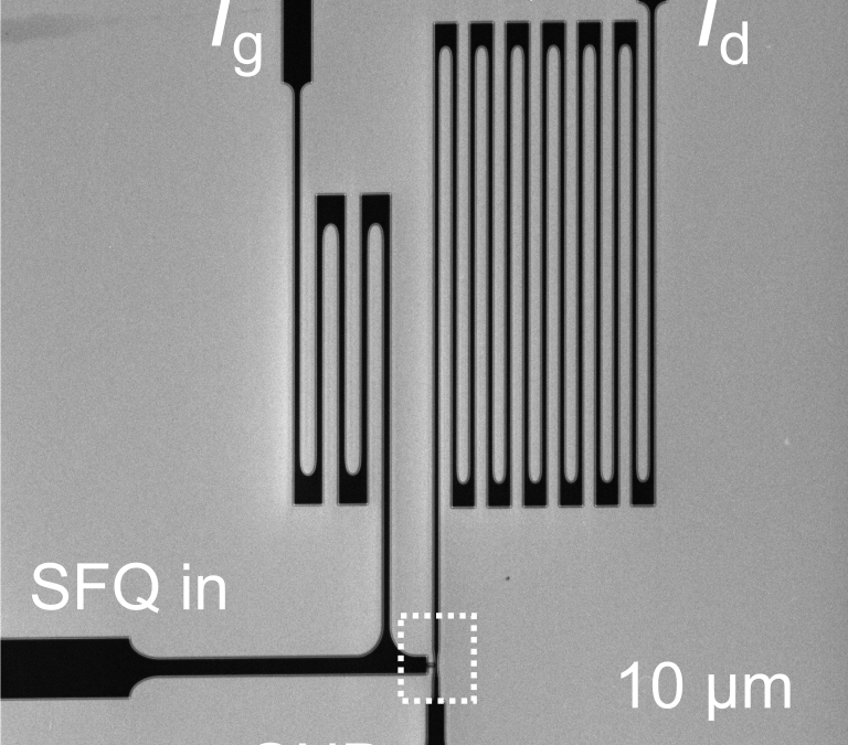
We demonstrate the use of a single three-terminal superconducting-nanowire device, called the nanocryotron (nTron), as a digital comparator to combine SFQ circuits with mature semiconductor circuits such as complementary metal oxide semiconductor (CMOS) circuits....
Dec 21, 2016 | News Articles, Uncategorized
We demonstrate strong-field, carrier-envelope-phase-sensitive photoemission from arrays of tailored metallic nanoparticles, and we show the influence of the nanoparticle geometry and the plasmon resonance on the phase-sensitive response. Additionally, from a...
Sep 16, 2016 | News Articles, Uncategorized
Developing superconducting-nanowire based electronics We are looking for a graduate research assistant (must be an admitted MIT graduate student) to develop novel quantum sensors, logic devices and digital circuits based on superconducting nanowires. Present projects...
Mar 21, 2016 | News Articles, Our Research
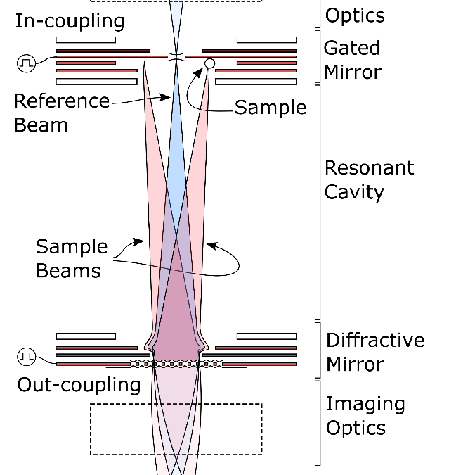
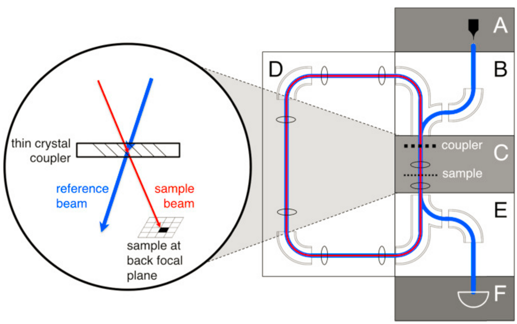
One of the astounding consequences of quantum mechanics is that it allows the detection of a target using an incident probe, with only a low probability of interaction of the probe and the target. This ‘quantum weirdness’ could be applied in the field of electron...
Jan 13, 2016 | News Articles
Hydrothermally synthesized ZnO nanowire arrays are critical components in a range of nanostructured semiconductor devices. The device performance is governed by relevant nanowire morphological parameters that cannot be fully controlled during bulk hydrothermal...

Aug 4, 2015 | News Articles
A showcase of MTL’s diverse and creative research, this report contains 147 abstracts submitted by 40 research groups. The QNN group’s contributions can be found here: Driving Stage for SFQ Circuits using a Single Nanocryotron Modeling Superconducting...
Jun 19, 2015 | News Articles
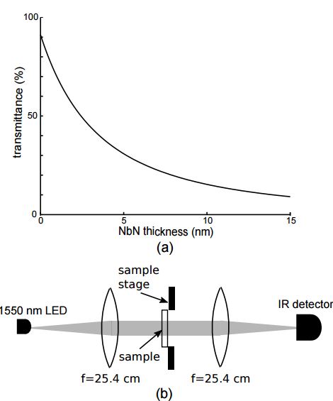
We built a transmissometer to determine the thickness of thin films of NbN that are deposited as the starting material for SNSPDs. The transmissometer measures the transmittance of light through NbN thin films, and the thickness of the NbN is found by fitting the...