Feb 3, 2015 | News Articles, Our Research
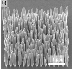
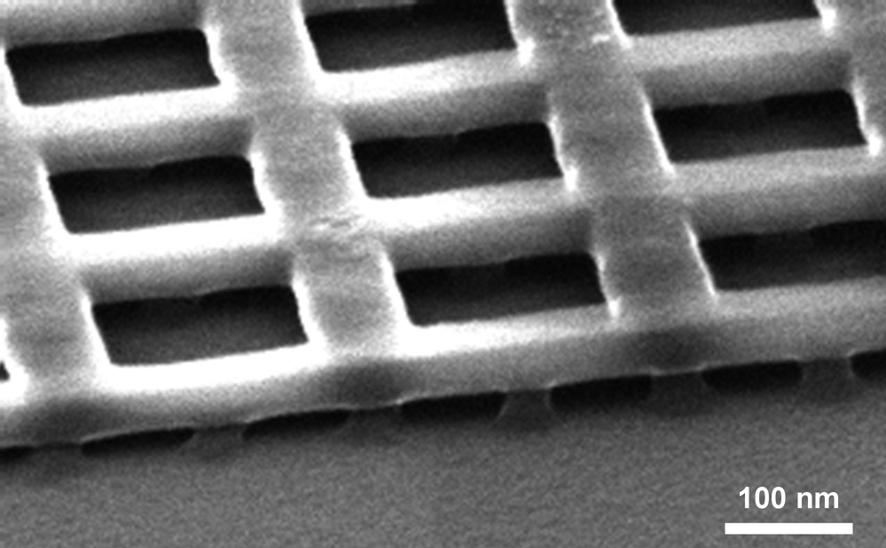
[abstract] We found that electron-beam lithography, a top-down approach, is a suitable prototyping method for templating and controlling hydrothermally-grown ZnO nanowires (NWs). By varying the deposition method of the ZnO seed layer, annealing and template hole...
Jan 7, 2015 | News Articles, Our Research
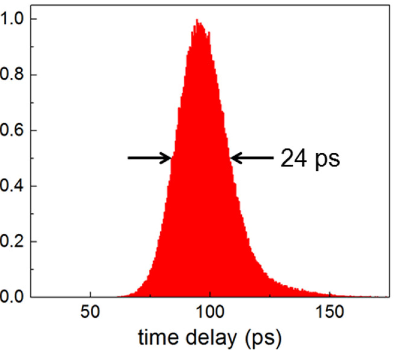
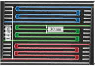
In our new paper, to appear in the IEEE Jornal of Selected Topics in Quantum Electronics (JSTQE), we have demonstrated fully-saturated nanowire single-photon detectors with 24 ps jitter. Furthermore we show an improved fabrication process that allowed us to increase...
Dec 17, 2014 | News Articles, Our Research
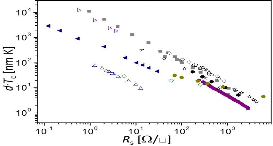
[preprint] [supp. info.] We reported that the superconducting properties scale universally close to the superconducting-to-insulating transition in thin films. This universal behavior was found useful not only for the fundamental understanding of superconductivity...
Nov 11, 2014 | News Articles, Our Research
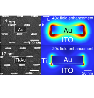
[abstract] Here we demonstrate the design, fabrication and characterization of ultrafast, surface-plasmon enhanced Au nanorod optical field emitter arrays. We present a quantitative study of electron emission from Au nanorod arrays fabricated by high-resolution...
Sep 29, 2014 | News Articles
Congrats to Hyung Wan Do on his recent paper being chosen as an editor’s pick in JVST B. Editor’s Pick
Sep 8, 2014 | Our Research
We design and fabricate superconducting nanowire single photon detectors (SNSPDs). SNSPDs are appropriate for many applications because they have low jitter, a fast reset time and good sensitivity to infrared light. Thus, we are working on several research projects to...

Aug 28, 2014 | Our Research
Nanofabrication, and nanolithography in particular, are the cornerstone of the modern microelectronics industry, and are integral to the future of nanotechnology as a whole. We are investigating fundamental challenges associated with continued scaling of electronic...
Mar 26, 2013 | News Articles
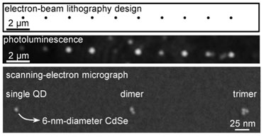
Nanotechweb has released a Journal Highlight of some of our recently published work. The research involves using electron beam lithography to precisely place quantum dots on a sample surface. The work explores size and height of different templating holes in a PMMA...