Nanofabrication, and nanolithography in particular, are the cornerstone of the modern microelectronics industry, and are integral to the future of nanotechnology as a whole. We are investigating fundamental challenges associated with continued scaling of electronic and nano-photonic device components. We are investigating the resolution limits of charged-particle lithography, including electron-beam and ion-beam lithography. The group also actively investigates the use of nanostructure arrays fabricated by nanolithography, as templates for: self-assembly of block copolymers, placement control of biomolecules or quantum dots, and as sources for the production of coherent electron pulses.
Continued scaling of devices toward molecular dimensions continues to unearth fascinating physical phenomena, which are of fundamental scientific interest as well as being critical to the development of future applications.
Charged Particle Lithography
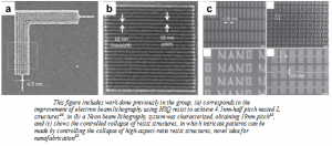
For several years now, the group has worked on novel nanofabrication technologies to push the boundaries of the electronics industry well into the nanotechnology regime (sub-100 nm)[42, 48, 66], and charge particle lithography (CPL) is a big part of this effort. The work done has ranged from improving the resolution limits of resists for CPL (HSQ and PMMA) [80, 87] to the development and characterization of new lithography systems (Helium and Neon Ion Beam Lithography). Important and exhaustive studies have been developed to understand the fundamental limits of CPL (acceleration voltage[85], beam spot size, charged particle used[67, 88], resist[80, 87], etc.). This group is now working on improved ways to implement the knowledge obtained to increase the resolution[89], yield, quality of nanofabrication, and the use of this nanofabrication to different areas of electronic research.
Templated Self-Assembly
The group has focussed considerably on the use of high-resolution nanofabrication for the direction of many different self assembly systems. The templated-self assembly of block copolymer thin films has been an area of significant investigation and interest over the past few years. Work has focussed on the PS-b-PDMS polymer of many different morphologies and templating mechanisms. The group has achieved complex and long-range control as reported in many different papers[53, 70, 71]. The templating of other self-assembly systems is of interest and future research.
42. “Enhancing etch resistance of hydrogen silsesquioxane via postdevelop electron curing,” Joel K. W. Yang, Vikas Anant, and Karl K. Berggren, Journal of Vacuum Science and Technology B 24, 3157 (2006)
48. “Using high-contrast salty development of hydrogen silsesquioxane for sub-10-nm half-pitch lithography,” Joel K. W. Yang and Karl K. Berggren, Journal of Vacuum Science and Technology B25, 2025 (2007)
53. “Graphoepitaxy of Self-Assembled Block Copolymers on Two-Dimensional Periodic Patterned Templates,” Ion Bita, Joel K. W. Yang, Yeon Sik Jung, Caroline A. Ross, Edwin L. Thomas, and Karl K. Berggren, Science 321, 939 (2008).
58. “Si-Containing Block Copolymers for Self-Assembled Nanolithography (invited),” C.A. Ross, Y.S. Jung, V.P.Chuang, F. Ilievski, J.K.W. Yang, I. Bita, E.L. Thomas, H.I. Smith, K.K. Berggren, J.G.Vansco, and J.Y. Cheng, Journal of Vacuum Science and Technology B 26, pp.2489-2494 (2008)
66. “Understanding of Hydrogen Silsesquioxane Electron Resist for Sub-5-nm-Half-Pitch Lithography,” Joel K.W. Yang, Bryan Cord, Karl K. Berggren, Joseph Klingfus, Sung-Wook Nam, Ki-Bum Kim, and Michael J. Rooks, Journal of Vacuum Science and Technology B 27, pp. 2622-2627 (2009).
67. “Scanning-helium-ion-beam lithography with hydrogen silsesquioxane resist,” D. Winston, B. M. Cord, B. Ming, D. C. Bell, W. F. DiNatale, L. A. Stern, A. E. Vladar, M. T. Postek, M. K. Mondol, J. K. W. Yang, and K. K. Berggren, Journal of Vacuum Science and Technology B 27, pp. 2702-2706
(2009).
70. “A Path to Ultranarrow Patterns Using Self-Assembled Lithography,” Yeon Sik Jung, J. B. Chang, Eric Verploegen, Karl K. Berggren and C. A. Ross, Nano Letters 10, pp. 1000-1005 (2010)
71. “Complex self-assembled patterns using sparse commensurate templates with locally varying motifs,” Joel K. W. Yang, Yeon Sik Jung, Jae-Byum Chang, R. A. Mickiewicz, A. Alexander-Katz, C. A. Ross and Karl K. Berggren, Nature Nanotechnology 5, pp. 256-260 (2010).
80. “Sub-10-nm Half-Pitch Electron-Beam Lithography by Using PMMA as a Negative Resist,” Huigao Duan, Donald Winston, Joel K. W. Yang, Bryan M. Cord, Vitor R. Manfrinato, and Karl K. Berggren, Journal of Vacuum Science and Technology B 28 C6C58-C6C62 (2010).
85. “Sub-5 keV Electron-Beam Lithography in Hydrogen Silsesquioxane Resist,” Vitor R. Manfrinato, Lin Lee Cheong, Huigao Duan, Donald Winston, Henry I. Smith, Karl K. Berggren, Journal of Microelectronic Engineering To be published (2011).
87. “Electrochemical development of hydrogen silsesquioxane by applying an electrical potential,” Sebastian Strobel, Katherine J Harry, Huigao Duan, Joel K W Yang, Vitor R Manfrinato and Karl K Berggren, Nanotechnology 22 375301(2011).
88. “Neon Ion Beam Lithography (NIBL),” Donald Winston , Vitor R Manfrinato , Samuel M Nicaise, Lin Lee Cheong , Huigao Duan , David Ferranti , Jeff Marshman , Shawn McVey , Lewis A Stern, John A Notte , and Karl Berggren, Nano Letters Available Online(2011).
89. “Controlled Collapse of High-Aspect-Ratio Nanostructures,” Huigao Duan, Joel K. W. Yang, and Karl K. Berggren, Small, 7, No. 18, 2661-2668 (2011).

