News
New Publication “Design and characterization of superconducting nanowire-based processors for acceleration of deep neural network training”
Training of deep neural networks (DNNs) is a computationally intensive task and requires massive volumes of data transfer. Performing these operations with the conventional von Neumann architectures creates unmanageable time and power costs. Recent studies have shown that mixed-signal designs involving resistive crossbar architectures are capable of achieving acceleration factors as high as 30 000 × over the state of the art digital processors. These approaches involve utilization of non-volatile memory elements as local processors. However, no technology has been developed to-date that can satisfy the strict device requirements for the unit cell. This paper presents the superconducting nanowire-based processing element as a crosspoint device. The unit cell has many programmable non-volatile states that can be used to perform analog multiplication. Importantly, these states are intrinsically discrete due to quantization of flux, which provides symmetric switching characteristics. Operation of these devices in a crossbar is described and verified with electro-thermal circuit simulations. Finally, validation of the concept in an actual DNN training task is shown using an emulator.
A complete description of the work may be found here.
New Publication “Detecting Sub-GeV Dark Matter with Superconducting Nanowires”
We propose the use of superconducting nanowires as both target and sensor for direct detection of sub-GeV dark matter. With excellent sensitivity to small energy deposits on electrons and demonstrated low dark counts, such devices could be used to probe electron recoils from dark matter scattering and absorption processes. We demonstrate the feasibility of this idea using measurements of an existing fabricated tungsten-silicide nanowire prototype with 0.8-eV energy threshold and 4.3 ng with 10 000 s of exposure, which showed no dark counts. The results from this device already place meaningful bounds on dark matter-electron interactions, including the strongest terrestrial bounds on sub-eV dark photon absorption to date. Future expected fabrication on larger scales and with lower thresholds should enable probing of new territory in the direct detection landscape, establishing the complementarity of this approach to other existing proposals.
A complete description of the work may be found here.
New Publication “Investigation of ma-N 2400 series photoresist as an electron-beam resist for superconducting nanoscale devices”
Superconducting nanowire-based devices are increasingly being used in complex circuits for applications such as photon detection and amplification. To keep up with the growing circuit complexity, nanowire processing is moving from single layer fabrication to heterogeneous multilayer processes. Hydrogen silsesquioxane (HSQ) is the most common choice of negative-tone electron-beam resist for patterning superconducting nanowires. However, HSQ has several limitations, including an inability to be removed without a strong reagent that damages the superconducting film, making it unsuitable for multilayer fabrication. As a result, it is vital to consider alternative resists that can be removed through less harmful solvents. Here, the authors explore the use of ma-N 2400 series deep ultraviolet photoresist as an electron-beam resist for fabricating superconducting nanowire devices. They demonstrate that ma-N can be used to pattern dense lines as narrow as 30 nm and isolated features below 20 nm in width. They also examine the reproducibility of 36 identical superconducting devices by comparing their minimum dimensions and switching currents. Through this analysis, they conclude that ma-N 2400 is a suitable electron-beam resist for fabricating nanoscale devices and has the potential to expand the use of nanowire-based technologies into more advanced applications.
A complete description of the work may be found here.
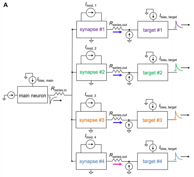
New Publication “Design of a Power Efficient Artificial Neuron Using Superconducting Nanowires”
With the rising societal demand for more information-processing capacity with lower power consumption, alternative architectures inspired by the parallelism and robustness of the human brain have recently emerged as possible solutions. In particular, spiking neural networks (SNNs) offer a bio-realistic approach, relying on pulses, analogous to action potentials, as units of information. While software encoded networks provide flexibility and precision, they are often computationally expensive. As a result, hardware SNNs based on the spiking dynamics of a device or circuit represent an increasingly appealing direction. Here, we propose to use superconducting nanowires as a platform for the development of an artificial neuron. Building on an architecture first proposed for Josephson junctions, we rely on the intrinsic non-linearity of two coupled nanowires to generate spiking behavior, and use electrothermal circuit simulations to demonstrate that the nanowire neuron reproduces multiple characteristics of biological neurons. Furthermore, by harnessing the non-linearity of the superconducting nanowire’s inductance, we develop a design for a variable inductive synapse capable of both excitatory and inhibitory control. We demonstrate that this synapse design supports direct fan-out, a feature that has been difficult to achieve in other superconducting architectures, and that the nanowire neuron’s nominal energy performance is competitive with that of current technologies.
A complete description of the work may be found here.
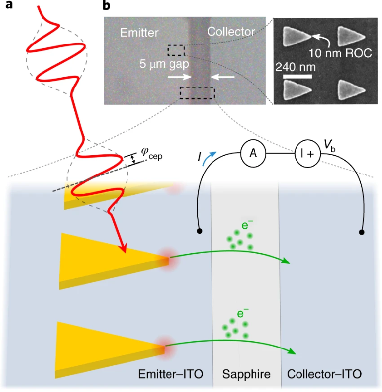
New Publication “Vanishing carrier-envelope-phase-sensitive response in optical-field photoemission from plasmonic nanoantennas”
At the surfaces of nanostructures, enhanced electric fields can drive optical-field photoemission and thereby generate and control electrical currents at frequencies exceeding 100 THz. A hallmark of such optical-field photoemission is the sensitivity of the total emitted current to the carrier-envelope phase (CEP). Here, we examine CEP-sensitive photoemission from plasmonic gold nanoantennas excited with few-cycle optical pulses. At a critical pulse energy, which we call a vanishing point, we observe a pronounced dip in the magnitude of the CEP-sensitive photocurrent accompanied by a sudden shift of π radians in the photocurrent phase. Analysis shows that this vanishing behaviour arises due to competition between sub-optical-cycle electron emission events from neighbouring optical half-cycles and that both the dip and phase shift are highly sensitive to the precise shape of the driving optical waveform at the surface of the emitter. As the mechanisms underlying the dip and phase shift are a general consequence of nonlinear, field-driven photoemission, they may be used to probe sub-optical-cycle emission processes from solid-state emitters, atoms and molecules. Improved understanding of these CEP-sensitive photocurrent features will be critical to the development of optical-field-driven photocathodes for time-domain metrology and microscopy applications demanding attosecond temporal and nanometre spatial resolution.
A complete description of the work may be found here.