News
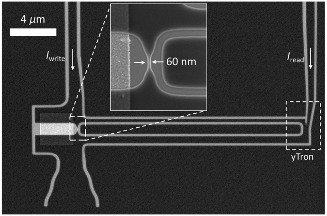
New Publication “Bridging the Gap Between Nanowires and Josephson Junctions: A Superconducting Device Based on Controlled Fluxon Transfer”
The basis for superconducting electronics can broadly be divided between two technologies: the Josephson junction and the superconducting nanowire. While the Josephson junction (JJ) remains the dominant technology due to its high speed and low power dissipation, recently proposed nanowire devices offer improvements such as gain, high fanout, and compatibility with CMOS circuits. Despite these benefits, nanowire-based electronics have largely been limited to binary operations, with devices switching between the superconducting state and a high-impedance resistive state dominated by uncontrolled hotspot dynamics. Unlike the JJ, they cannot increment an output through successive switching and their operation speeds are limited by their slow thermal-reset times. Thus, there is a need for an intermediate device with the interfacing capabilities of a nanowire but a faster, moderated response allowing for modulation of the output. We present a nanowire device based on controlled fluxon transport. We show that the device is capable of responding proportionally to the strength of its input, unlike other nanowire technologies. The device can be operated to produce a multilevel output with distinguishable states, the number of which can be tuned by circuit parameters. Agreement between experimental results and electrothermal circuit simulations demonstrates that the device is classical and may be readily engineered for applications including use as a multilevel memory.
A complete description of the work may be found here.
New Publication “Design and Simulation of a Linear Electron Cavity for Quantum Electron Microscopy”
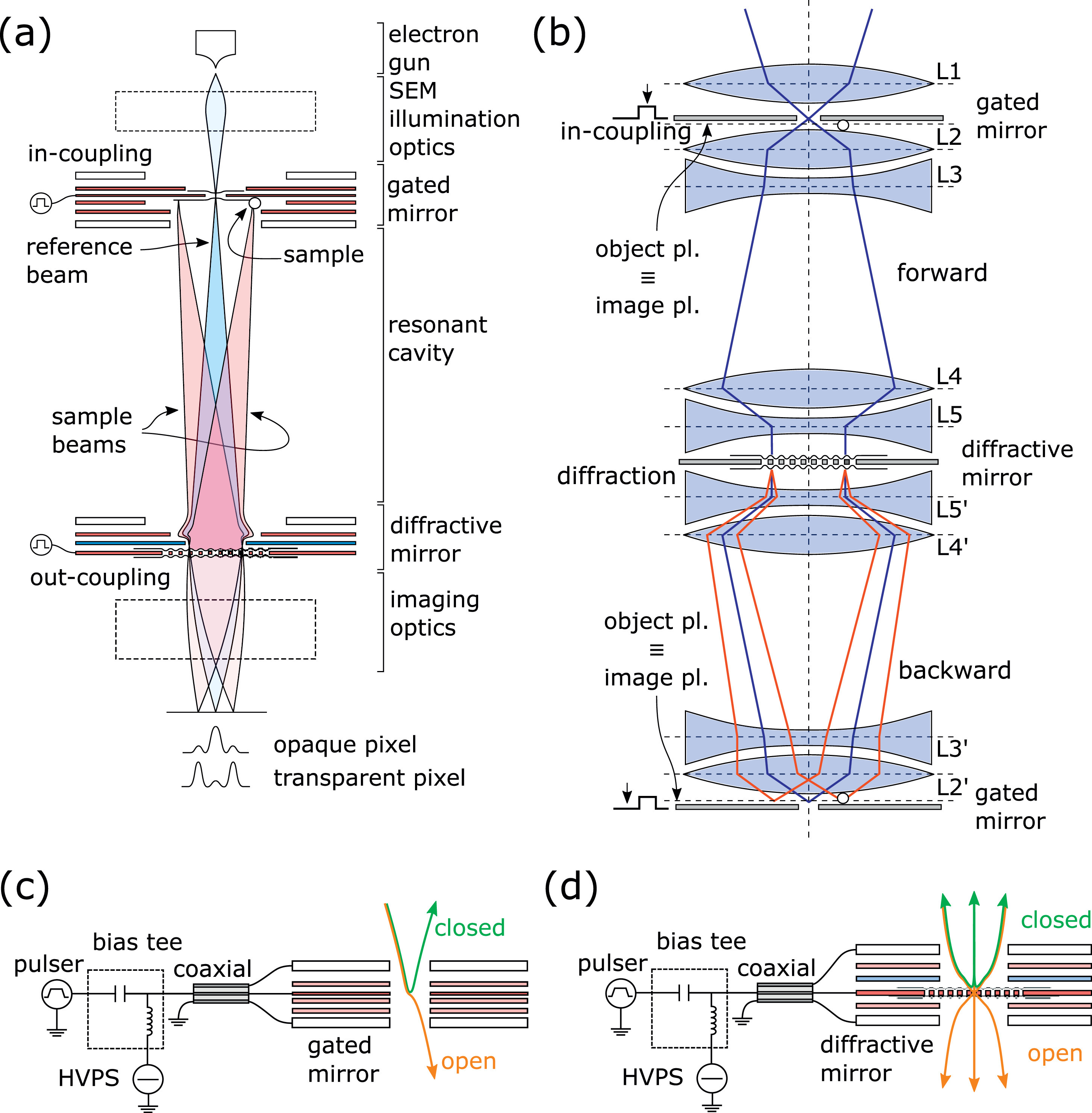
Quantum electron microscopy (QEM) is a measurement approach that could reduce sample radiation damage, which represents the main obstacle to sub-nanometer direct imaging of molecules in conventional electron microscopes. This method is based on the exploitation of interaction-free measurements in an electron resonator. In this work, we present the design of a linear resonant electron cavity, which is at the core of QEM. We assess its stability and optical properties during resonance using ray-tracing electron optical simulations. Moreover, we analyze the issue of spherical aberrations inside the cavity and we propose and verify through simulation two possible approaches to the problem. Finally, we discuss some of the important design parameters and constraints, such as conservation of temporal coherence and effect of alignment fields.
A complete description of the work may be found here.
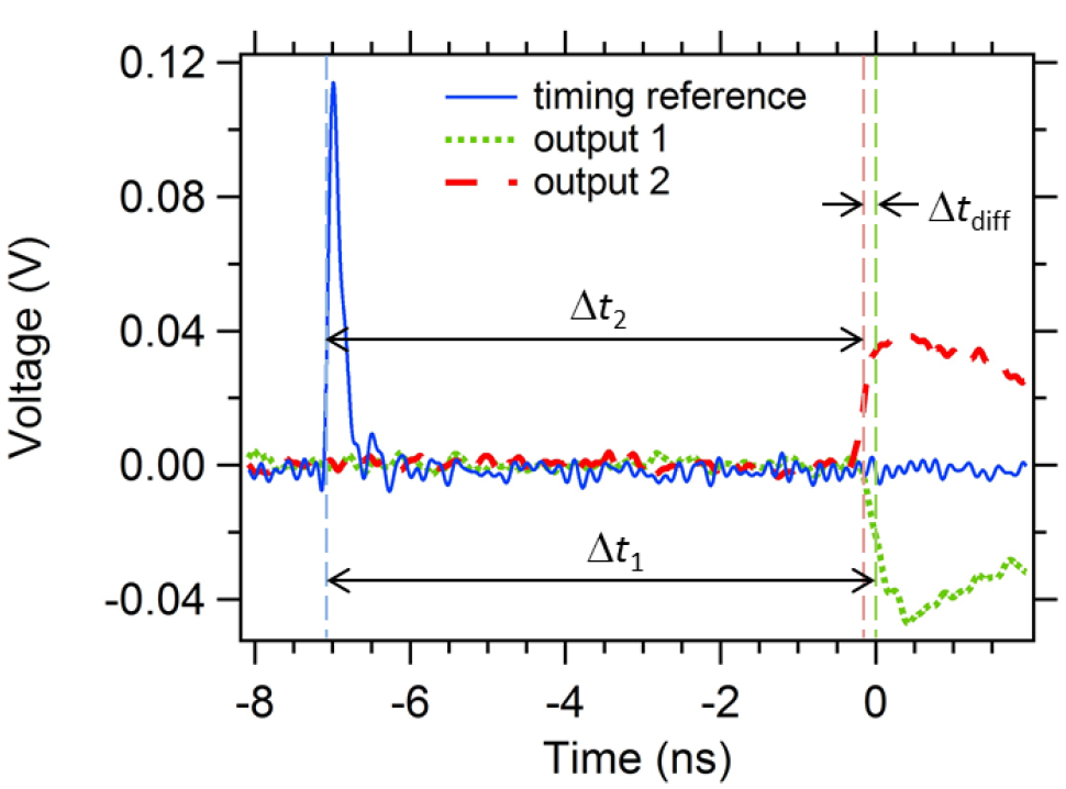
New Publication “Jitter Characterization of a Dual-Readout SNSPD”
To better understand the origins of the timing resolution, also known as jitter, of superconducting nanowire single photon detectors (SNSPDs), we have performed timing characterizations of a niobium nitride SNSPD with a dual-ended readout. By simultaneously measuring both readout pulses along with an optical timing reference signal, we are able to quantify each independent contribution to the total measured jitter. In particular, we are able to determine values for the jitter due to the stochastic nature of hotspot formation and the jitter due to the variation of the photon detection location along the length of the nanowire. We compare the results of this analysis for measurements at temperatures of 1.5 K and 4.5 K.
A complete description of the work may be found here.
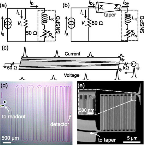
New Publication “Superconducting nanowire single-photon detector with integrated impedance-matching taper”
Conventional readout of a superconducting nanowire single-photon detector (SNSPD) sets an upper bound on the output voltage to be the product of the bias current and the load impedance, IB × Zload, where Zload is limited to 50 Ω in standard r.f. electronics. Here, we break this limit by interfacing the 50 Ω load and the SNSPD using an integrated superconducting transmission line taper. The taper is a transformer that effectively loads the SNSPD with high impedance without latching. At the expense of reduced maximum counting rate, it increases the amplitude of the detector output while preserving the fast rising edge. Using a taper with a starting width of 500 nm, we experimentally observed a 3.6× higher pulse amplitude, 3.7× faster slew rate, and 25.1 ps smaller timing jitter. The results match our numerical simulation, which incorporates both the hotspot dynamics in the SNSPD and the distributed nature in the transmission line taper. The taper studied here may become a useful tool to interface high-impedance superconducting nanowire devices to conventional low-impedance circuits.
A complete description of the work may be found here.
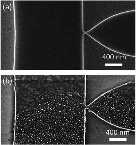
New Publication “Influence of tetramethylammonium hydroxide (TMAH) on niobium nitride thin films”
Functionality of superconducting thin-film devices such as superconducting nanowire single photon detectors stems from the geometric effects that take place at the nanoscale. The engineering of these technologies requires high-resolution patterning, often achieved with electron beam lithography. Common lithography processes using hydrogen silsesquioxane (HSQ) as the electron beam resist rely on tetramethylammonium hydroxide (TMAH) as both a developer and a resist adhesion promoter. Despite the strong role played by TMAH in the fabrication of superconducting devices, its potential influence on the superconducting films themselves has not yet been reported. In this work, the authors demonstrate that a 25% TMAH developer damages niobium nitride (NbN) thin films by modifying the surface chemistry and creating an etch contaminant that slows reactive ion etching in CF4. They also show how the identity of the contaminant may be revealed through characterization including measurement of the superconducting film properties and Fourier transform infrared spectroscopy. Although workarounds may be available, the results reveal that processes using 25% TMAH as an adhesion promoter are not preferred for NbN films and that changes to the typical HSQ fabrication procedure will need to be made in order to prevent damage of NbN nanoscale devices.
A complete description of the work may be found here.